

For a collector follower with emitter resistor, you’ll often find that the gain per stage is no more than 10 to 50 times. The gain increases when the emitter resistor is omitted. Unfortunately, the distortion also increases. With a ubiquitous transistor such as the BC547B, the gain of the transistor is roughly equal to 40 times the collector current (Ic), provided the collector current is less than a few milliamps. This value is in theory equal to the expression q/KT, where q is the charge of the electron, K is Boltzmann’s constant and T is the temperature in Kelvin.
For simplicity, and assuming room temperature, we round this value to 40. For a single stage amplifier circuit with grounded emitter it holds that the gain Uout /Uin (for AC voltage) is in theory equal to SRc. As we observed before, the slope S is about 40Ic. From this follows that the gain is approximately equal to 40I cRc. What does this mean? In the first instance this leads to a very practical rule of thumb: that gain of a grounded emitter circuit amounts to 40·I c·Rc, which is equal to 40 times the voltage across the collector resistor.
If Ub is, for example, equal to 12 V and the collector is set to 5V, then we know, irrespective of the values of the resistors that the gain will be about 40R(12–5) = 280. Notable is the fact that in this way the gain can be very high in theory, by selecting a high power supply voltage. Such a voltage could be obtained from an isolating transformer from the mains. An isolating transformer can be made by connecting the secondaries of two transformers together, which results in a galvanically isolated mains voltage.
For simplicity, and assuming room temperature, we round this value to 40. For a single stage amplifier circuit with grounded emitter it holds that the gain Uout /Uin (for AC voltage) is in theory equal to SRc. As we observed before, the slope S is about 40Ic. From this follows that the gain is approximately equal to 40I cRc. What does this mean? In the first instance this leads to a very practical rule of thumb: that gain of a grounded emitter circuit amounts to 40·I c·Rc, which is equal to 40 times the voltage across the collector resistor.
If Ub is, for example, equal to 12 V and the collector is set to 5V, then we know, irrespective of the values of the resistors that the gain will be about 40R(12–5) = 280. Notable is the fact that in this way the gain can be very high in theory, by selecting a high power supply voltage. Such a voltage could be obtained from an isolating transformer from the mains. An isolating transformer can be made by connecting the secondaries of two transformers together, which results in a galvanically isolated mains voltage.
10,000x With One Transistor Circuit diagram:
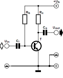
That means, that with a mains voltage of 240 Veff there will be about 340 V DC after rectification and filtering. If in the amplifier circuit the power supply voltage is now 340 V and the collector voltage is 2 V, then the gain is in theory equal to 40 x (340–2). This is more than 13,500 times! However, there are a few drawbacks in practice. This is related to the output characteristic of the transistor. In practice, it turns out that the transistor does actually have an output resistor between collector and emitter.
This output resistance exists as a transistor parameter and is called ‘hoe’. In normal designs this parameter is of no consequence because it has no noticeable effect if the collector resistor is not large. When powering the amplifier from 340 V and setting the collector current to 1 mA, the collector resistor will have a value of 338 k. Whether the ‘hoe’-parameter has any influence depends in the type of transistor. We also note that with such high gains, the base-collector capacitance in particular will start to play a role.
As a consequence the input frequency may not be too high. For a higher bandwidth we will have to use a transistor with small Cbc, such as a BF494 or perhaps even an SHF transistor such as a BFR91A. We will have to adjust the value of the base resistor to the new hfe. The author has carried out measurements with a BC547B at a power supply voltage of 30 V. A value of 2 V was chosen for the collector voltage. Measurements confirm the rule of thumb. The gain was more than 1,000 times and the effects of ‘hoe’ and the base-collector capacitance were not noticeable because of the now much smaller collector resistor.
This output resistance exists as a transistor parameter and is called ‘hoe’. In normal designs this parameter is of no consequence because it has no noticeable effect if the collector resistor is not large. When powering the amplifier from 340 V and setting the collector current to 1 mA, the collector resistor will have a value of 338 k. Whether the ‘hoe’-parameter has any influence depends in the type of transistor. We also note that with such high gains, the base-collector capacitance in particular will start to play a role.
As a consequence the input frequency may not be too high. For a higher bandwidth we will have to use a transistor with small Cbc, such as a BF494 or perhaps even an SHF transistor such as a BFR91A. We will have to adjust the value of the base resistor to the new hfe. The author has carried out measurements with a BC547B at a power supply voltage of 30 V. A value of 2 V was chosen for the collector voltage. Measurements confirm the rule of thumb. The gain was more than 1,000 times and the effects of ‘hoe’ and the base-collector capacitance were not noticeable because of the now much smaller collector resistor.
Author: Gert Baars Copyright: Elektor Electronics


