
The schema diagram shows a low-cost 3-input video MUX cable driver. In this schema, the amplifier is loaded by the sum of RF and RG of each disabled amplifier. Resistor values have been chosen to keep the total back termination at 75 Ω while maintaining a gain of 1 at the 75-Ω load. The switching time between any two channels is approximately 32 ns when both enable pins are driven. When designing a schema board for this cable driver, care should be taken to minimize trace lengths at the inverting input. The ground plane should also be pulled away from RF and RG on both sides of the board to minimize stray capacitance. Current consumption of the cable driver is a modest 8mA.
Showing posts with label 3. Show all posts
Showing posts with label 3. Show all posts
Thursday, November 20, 2014
Mini Amplifier with 3 Transistor
Mini 3 transistor amplifier is a simple amplifier with 50mW power drawn by 3 transitor.
The series of three mini-amplifier transistors can be used for loud speaker 8 ohm load. Source voltage required to activate the mini-amplifier can be drawn from the batteries 9V.Rangkaian 3 transistor amplifier is often used in simple portabe audio devices such as radios or small tape recorder. Mini-transistor amplifier circuit 3 is quite simple as shown in the figure below.

Mini-transistor amplifier circuit 3 includes type of amplifier OTL (Output Transformer Less). Mini-transistor amplifier circuit 3 is used for output coupling capacitors. Amplifier circuit is simple and suitable when used for audio amplifier experiment.
Read More..
The series of three mini-amplifier transistors can be used for loud speaker 8 ohm load. Source voltage required to activate the mini-amplifier can be drawn from the batteries 9V.Rangkaian 3 transistor amplifier is often used in simple portabe audio devices such as radios or small tape recorder. Mini-transistor amplifier circuit 3 is quite simple as shown in the figure below.
Mini-transistor amplifier circuit 3 includes type of amplifier OTL (Output Transformer Less). Mini-transistor amplifier circuit 3 is used for output coupling capacitors. Amplifier circuit is simple and suitable when used for audio amplifier experiment.
Sunday, November 2, 2014
3 Way Crossover Speaker Circuit
Design simply what best fit the drivers capabilities while focusing on keeping the woofer in doing its job handling the bass, the mids handling the full midrange and so on. 500Hz and 4000Hz were chosen as the crossover frequencies. An L-pad circuit I felt was essential in keeping the response of the speaker perfect as possible. I didnt want anything to stick out. A schematic of the Hi-Vi 3 way crossover design is shown below.
 |
| 3 Way Crossover Speaker Circuit Diagram |
Friday, October 17, 2014
lm317 3 3 v schematic diagram
lm317 3.3 v schematic diagram
 The more expensive LM117 uses a 240 ohm resistor for R1. The LM317 is supposed to use a 120 om resistor or less so that its output voltage doesnt rise without a load if it has its max rated operating current and if its input voltage is high.
With 120 ohms for R1 and 360 ohms for R2 the output is 5.0V.
with 120 ohms for R1 and 200 ohms for R2 the output voltage is 3.333V.These resistors are common 5% values.
Read More..

With 120 ohms for R1 and 360 ohms for R2 the output is 5.0V.
with 120 ohms for R1 and 200 ohms for R2 the output voltage is 3.333V.These resistors are common 5% values.
Sunday, September 7, 2014
3 Way Active Crossover Wiring diagram Schematic
This is the Simple 3-Way Active Crossover Circuit Diagram with linear phase response. The problems that exist at common crossover schema is known. The low pass filter causes a delay in the signal. Unlike the high-pass filter causes a head in the signal passing through it. Thus the frequency separation created some problems such as:
- Signals of the two filters are mutually exclusive
- The phase shift between the filter affects the radiation
- The radiation pattern depends on the frequency
The crossover schema tries to solve many of the problems mentioned above and based on a study of S. Lipshitz and J. Vanderkooy, published in the JAES (Journal Audio Engineering Society). A lattice separation uses a linear phase low-pass section with the help of a time delay schema and a schema removal gives the output signal with high-pass filter characteristics. The time delay is not constant over the entire frequency range, but changing very slowly and mainly there are phase differences between signals of the two charges, not even close to the crossover.
Simple 3-Way Active Crossover Circuit Diagram
The schema consists separation as shown in block diagram [Fig.2] two low pass filters of fourth grade, -24db/oct for a line of low-frequency signals and one for the high frequency separation. In the same frequencies operate both units delay time T1 (for low frequency F1) and T2 (for high frequency F2) and give the same phase characteristics of the low pass section.

The delay schema T1 simulates the time delay introduced by low-frequency filter LPF1, while T2 simulates the time delay introduced by low-frequency filter LPF2 that exists in the line of midrange. Then the signal from the low pass filter removed [IC7A-B] of the signal has been delayed, a clear signal that the characteristics are the same as a signal that has passed through a high pass filter. At the exit of each line is a trimmer with which we can adjust the level between the levels of loudspeakers. The power schema is a well-stabilized voltage + /-15V. The use of meshed split fourth order Linkwitz forcing crossovers be located at-6db [Fig.3].

The above picture shows the main diagram and the necessary formulas for calculating the low pass filters as well as trusses time delay. There is also an example calculation for crossovers and 200IZ 3KIZ that will help calculate and adjust to your needs. The schema derived from a relevant article of the magazine Elektor.
Components List:
R1,16 = 100Kohms
R2,3,4,5 = 56Kohms
R6,27 = 37.5Kohms[33K+4.7K]
R8,9,12,13,14 = 10Kohms
R10,28 = 75Kohms (150K//150K)
R11,29 = NC
R15 = 56.3Kohms
R17 = 12Kohms
R18,19,20,21,22 = 10Kohms
R23,24,25,26 = 37.5Kohms [33K+4.7K]
R30,31,32,33,34,35,36 = 10Kohms
R37,38,39,40,41,41 = 10Kohms
R42,43,44 = 47Kohms
R45,46 = 47 ohms
TR1,2,3,4 = 47Kohms trimmer or pot.
C1,34,35 = 2.2uF 100V MKT
C2,3,7,8,14,15,18 = 47nF 100V MKT
C4,5,6,9,10,11,16,17 = 10nF 100V MKT
C12,13,20,21,22 = 1nF 100V MKT
C19,23,24,30,31,32,33 = 47nF 100V MKT
C25,26,27,28,29 = 1nF 100V MKT
C36,37 = 1uF 100V MKT
C38,39 = 47uF 25V
IC1 = TL071
IC2,3,4,5,6,7 = TL072,NE5532
All the resistors is 1/4W 1% metal film
R1,16 = 100Kohms
R2,3,4,5 = 56Kohms
R6,27 = 37.5Kohms[33K+4.7K]
R8,9,12,13,14 = 10Kohms
R10,28 = 75Kohms (150K//150K)
R11,29 = NC
R15 = 56.3Kohms
R17 = 12Kohms
R18,19,20,21,22 = 10Kohms
R23,24,25,26 = 37.5Kohms [33K+4.7K]
R30,31,32,33,34,35,36 = 10Kohms
R37,38,39,40,41,41 = 10Kohms
R42,43,44 = 47Kohms
R45,46 = 47 ohms
TR1,2,3,4 = 47Kohms trimmer or pot.
C1,34,35 = 2.2uF 100V MKT
C2,3,7,8,14,15,18 = 47nF 100V MKT
C4,5,6,9,10,11,16,17 = 10nF 100V MKT
C12,13,20,21,22 = 1nF 100V MKT
C19,23,24,30,31,32,33 = 47nF 100V MKT
C25,26,27,28,29 = 1nF 100V MKT
C36,37 = 1uF 100V MKT
C38,39 = 47uF 25V
IC1 = TL071
IC2,3,4,5,6,7 = TL072,NE5532
All the resistors is 1/4W 1% metal film
Sourced by Elektor
Sunday, August 31, 2014
Saturday, August 23, 2014
3 3 5 Watt FM transmitter circuit
This is 3-3.5 Watt FM transmitter schema. With this power, it should be able to reach 3-5 KM distance. The frequency range is about 90-110 MHz.

Component list
| Part | Total Qty. | Description | |
| R1,R4,R14,R15 | 4 | 10K 1/4W Resistor | |
| R2,R3 | 2 | 22K 1/4W Resistor | |
| R5,R13 | 2 | 3.9K 1/4W Resistor | |
| R6,R11 | 2 | 680 Ohm 1/4W Resistor | |
| R7 | 1 | 150 Ohm 1/4W Resistor | |
| R8,R12 | 2 | 100 Ohm 1/4W Resistor | |
| R9 | 1 | 68 Ohm 1/4W Resistor | |
| R10 | 1 | 6.8K 1/4W Resistor | |
| C1 | 1 | 4.7pF Ceramic Disc Capacitor | |
| C2,C3,C4,C5,C7,C11,C12 | 7 | 100nF Ceramic Disc Capacitor | |
| C6,C9,C10 | 3 | 10nF Ceramic Disc Capacitor | |
| C8,C14 | 2 | 60pF Trimmer Capacitor | |
| C13 | 1 | 82pF Ceramic Disc Capacitor | |
| C15 | 1 | 27pF Ceramic Disc Capacitor | |
| C16 | 1 | 22pF Ceramic Disc Capacitor | |
| C17 | 1 | 10uF 25V Electrolytic Capacitor | |
| C18 | 1 | 33pF Ceramic Disc Capacitor | |
| C19 | 1 | 18pF Ceramic Disc Capacitor | |
| C20 | 1 | 12pF Ceramic Disc Capacitor | |
| C21,C22,C23,C24 | 4 | 40pF Trimmer Capacitor | |
| C25 | 1 | 5pF Ceramic Disc Capacitor | |
| L1 | 1 | 5 WDG, Dia 6 mm, 1 mm CuAg, Space 1 mm | |
| L2,L3,L5,L7,L9 | 5 | 6-hole Ferroxcube Wide band HF Choke (5 WDG) | |
| L4,L6,L8 | 3 | 1.5 WDG, Dia 6 mm, 1 mm CuAg, Space 1 mm | |
| L10 | 1 | 8 WDG, Dia 5 mm, 1 mm CuAg, Space 1 mm | |
| D1 | 1 | BB405, BB102 or equal (most varicaps with C = 2-20 pF [approx.]) | |
| Q1 | 1 | 2N3866 | |
| Q2,Q4 | 2 | 2N2219A | |
| Q3 | 1 | BF115 | |
| Q5 | 1 | 2N3553 | |
| U1 | 1 | 7810 Regulator | |
| MIC | 1 | Electret Microphone | |
| MISC | 1 | PC Board, Wire For Antenna, Heatsinks |
Source: electronic-lab.com
Friday, August 22, 2014
Inductorless 3 to 5 Volts Converter Wiring diagram Schematic
By configuring a comparator and a transistor to control the oscillator in a charge pump schema, you enable the pump to generate a regulated output of in principle any desired value. Charge pump ICs can either invert or double an input voltage (for example, 3 V to –3 V or 3 V to 6 V). The charge pump itself does not regulate the output voltage and one running off 3 V is not normally capable of generating intermediate output voltage levels like 5 V. However, by adding a comparator and a reference device, you can create arbitrary output levels like 5 V and regulate them as well.
Inductorless 3-to-5 Volts Converter Circuit Diagram
Charge pump IC1 (a MAX660) has an internal oscillator whose 45 kHz operation transfers charge from C1 to C2, causing the regulated output to rise.
When the feedback voltage (pin 3 of IC2) exceeds 1.18 V, the output of comparator IC2 (a MAX921) goes high, turning off the oscillator via T1. The comparator hysteresis (easily added on IC2) is zero here simply because no hysteresis is required in the control loop. The oscillator when enabled generates two cycles, which is sufficient to drive VOUT slightly above the desired level. Next, the feedback turns the oscillator off again.
The resulting output ripple will depend mainly on the input voltage and the output load current. Output ripple may be reduced at the expense of schema efficiency by adding a small resistor (say, 1 ?) in series with C1. You’ll find that ripple also depends on the value and ESR associated with C1 - smaller values of C1 transfer less charge to C2, producing smaller jumps in V OUT.
Source by : Streampowers
3 Watt Stereo Audio Amplifier

This very simple schema is ideal for small power audio applications like portable CD players or radio sets.The schema is designed strictly as per the datasheet and found to be working great.
The MAX9710 a stereo audio power amplifier IC capable of delivering 3Watts of out put to 4 Ohm loads. MAX9710 can be operated from a single 4.5V to 5.5V power supply , makes it ideal for hand held applications.The IC also features thermal overload protection.
Notes:
- Use a 5 V DC power supply for powering the schema.
- If you want to use a battery ,then use a 6V battery with a IN 4007 diode series to the positive terminal of it.The diode will drop 0.7 V and the IC will get the rated ~5V.This is just a safety recommendation .
- Assemble the schema on a good quality PCB or common board.
source: diagramtoday.com
Thursday, August 21, 2014
3 in 1 Flash Light
Want to avoid the problem of carrying three different flashlights to perform a test? Why don’t you try integrating Ultra Violet, Infra Red and visible light together in one flashlight? Read on to know more about this.
The multi-tasking flashlight is basically composed of a metallic case, a switch, cables and connections, four 9V batteries and three different LED heads that provide the desired light beam. For the construction of this flashlight, LedEngin’s LZ4-40 is recommended. This comes with a very wide wavelength that includes infra red and ultra violet light. Distinct visible light color temperature can also be found
The first step is to build the body of the flashlight, using an aluminum tube. Next come the drilling and cutting for switches and covers. Once the body is finished, the work on the constant current driver should be completed, adding the proper terminals for the batteries and the base for the LED heads.
The first step is to build the body of the flashlight, using an aluminum tube. Next come the drilling and cutting for switches and covers. Once the body is finished, the work on the constant current driver should be completed, adding the proper terminals for the batteries and the base for the LED heads.
Once all the power source wiring is completed and insulated with heat shrink tubing, the LED heads are assembled and connected. These are basically composed of an aluminum cap. The LED base and the power source connections come from the batteries.
Wednesday, August 20, 2014
3 Line Mixer
Actually, you can modify this schema become more than 3 lines mixer. Just add and repeat the input parts (P=10K R=22K).
Schematic diagram:

Component placement:

PCB layout:

Read More..
Schematic diagram:
Component placement:
PCB layout:
Monday, August 18, 2014
Mini Amplifier with 3 Transistor
Mini 3 transistor amplifier is a simple amplifier with 50mW power drawn by 3 transitor.
The series of three mini-amplifier transistors can be used for loud speaker 8 ohm load. Source voltage required to activate the mini-amplifier can be drawn from the batteries 9V.Rangkaian 3 transistor amplifier is often used in simple portabe audio devices such as radios or small tape recorder. Mini-transistor amplifier circuit 3 is quite simple as shown in the figure below.
![Mini]()
Mini-transistor amplifier circuit 3 includes type of amplifier OTL (Output Transformer Less). Mini-transistor amplifier circuit 3 is used for output coupling capacitors. Amplifier circuit is simple and suitable when used for audio amplifier experiment.
Read More..
The series of three mini-amplifier transistors can be used for loud speaker 8 ohm load. Source voltage required to activate the mini-amplifier can be drawn from the batteries 9V.Rangkaian 3 transistor amplifier is often used in simple portabe audio devices such as radios or small tape recorder. Mini-transistor amplifier circuit 3 is quite simple as shown in the figure below.
Mini-transistor amplifier circuit 3 includes type of amplifier OTL (Output Transformer Less). Mini-transistor amplifier circuit 3 is used for output coupling capacitors. Amplifier circuit is simple and suitable when used for audio amplifier experiment.
Wednesday, August 13, 2014
2 3 Watt Low audio power amplifier
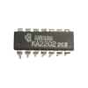
These amplifiers using IC KA2202 and KA2207, which has a power output of 2.3 Watt berimpedansi 4 ohms. Minimum supply voltage and maximum 5Volt 20Volt. See schematics and component list below.
Read more
Subscribe to:
Posts (Atom)
