Showing posts with label fm. Show all posts
Showing posts with label fm. Show all posts
Wednesday, November 19, 2014
TDA 7012T FM Radio Receiver
FM Radio Receiver IC TDA 7012T is very simple, but it has an FM radio receiver sensitivity and good selectivity. Single Chip FM Receifer cool name of IC TDA7012T 7012T TDA is to build an FM receiver requires a few additional components. Feature contained in FM receiver IC TDA 7012T is quite tempting to an FM receiver. Among features an FM receiver TDA 7012T is a low-voltage applications micro affability arrangement (MTS), Frequency Loked Loop (FLL) to 76 KHz range and selectivity of FM receiver with RC Filter. In an article by FM Radio Receiver IC TDA 7012T can be seen in the FM receiver circuit which can be made.
Image Series FM Radio Receiver with IC TDA 7012T

From the picture above components to make the FM Radio Receiver IC TDA 7012T as follows:
R1 = 8kΩ2
R2 = 10kΩ
R3 = 390Ω
C1, C3 = 10nF
C2, C6, C9, C16 = 100nF
C4 = 33pF
C5 = 25pF trimmer
C7, C10 = 1nF5
C8 = 820pF C11 = 1NF
C12 = 68pF
C13 = 220pF
C14 = 47μF 10V
C15 = 3nF3
L1 = 36nH
L2 = 1μH,
IC1 = TDA7021T
Hopefully useful and become an idea in the manufacture of Mini FM Receiver with IC TDA 7012T

Tuesday, November 18, 2014
Simple fm transmitter for the experiment
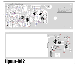
Simple fm transmitter for the experiment. This designation may be appropriate to call this series, because rangkaianya very simple and suitable for learning / beginners. and preferably when assembling, which assembled its first part oscilator. then we try it first. if able to function normally, we can proceed to the next level up to the booster.
Monday, September 22, 2014
Mini FM Receiver Circuit
Mini FM Receiver Circuit

This is a nearly complete integrated receiver circuit which has been specifically designed for portable radios and the like, requiring only a minimum of external components. As a result the final dimensions of the radio can be kept very small. The IC uses a frequency-locked-loop (FLL) system with an intermediate frequency of 76 kHz. The selectivity is obtained with the aid of active RC filters. The only ‘calibration’ adjustment in the circuit is the resonance frequency of the oscillator for the tuning.
The RF signal enters at pin 12 and is amplified first, after which it is transformed down by the mixer and passes through two IF filters. It is subsequently limited in amplitude. The IF limiter also supplies a signal for the optional signal strength indicator (via pin 9). The limited FM signal then goes to the demodulator and the correlator which decides whether the signal is tuned in properly. The demodulated are entirely available. This is also the reason that it is not recommended to connect the audio output directly to the line input of an audio system.
FM Receiver Circuit Schematic

The complete circuit for the FM receiver is shown above. The design is virtually identical to the test circuit shown in the datasheet for the IC, because this is difficult to improve even a little without adding a lot of additional electronics. Now we only need a few resistors and capacitors plus a coil. The tuning circuit
correctly covers the entire VHF FM broadcast band from 88 to 108 MHz. Tuning is done with trimmer capacitor C5.
There is also a connection (K2) for a simple signal strength meter. Via resistor R1 and decoupling capacitor C9, pin 9 supplies a DC voltage which is a measure of the received signal strength. At 170 μA the output current is too small to drive an LED, but you could connect an ‘oldfashioned’ moving coil meter. For the antenna you can use a simple wire antenna of about 75 cm long, which is soldered directly to the PCB.
FM Receiver Printed Circuit Board
SMD parts are used everywhere to keep the dimensions as small as possible. Soldering these small parts requires a bit of practice however. The dimensions of this tiny PCB are only 3.2 × 2.7 cm! The circuit contains no difficult coils, only the VCO requires an air-cored inductor with only 4 turns.

This receiver is a mono implementation, but at the output (as already mentioned) the entire multiplexed signal (up to 53 kHz) is available. By using a PLL stereo decoder, such as the TDA7040T, a stereo signal can be generated in a traightforward way from the output signal of the TDA7021T.
FM Receiver Circuit Parts List
Resistors (SMD 0805)
R1 = 8kΩ2
R2 = 10kΩ
R3 = 390Ω
Capacitors (SMD 0805)
C1,C3 = 10nF
C2,C6,C9,C16 = 100nF
C4 = 33pF
C5 = 25pF trimmer (Murata type TZB4Z250AB10R00)
C7,C10 = 1nF5
C8 = 820pF
C11 = 1nF
C12 = 68pF
C13 = 220pF
C14 = 47μF 10V (Nichicon UWX1A470MCL1GB 5.5mmL chip type)
C15 = 3nF3
Inductors
L1 = 36nH (4 turns 0.5mm silver-plated wire, inside diameter 4mm; length 7mm)
L2 = 1μH, SMD case 0805 (fres > 300 MHz)
Semiconductors
IC1 = TDA7021T (SMD in SO16 case)
Miscellaneous
K1,K2 = 2-way pinheader
BT1 = 2-way pinheader + battery holder for 2-4 AA batteries
Tuesday, September 9, 2014
Long range FM transmitter
The power output of most of these diagram are very low because no power amplifier stages were incorporated.
The transmitter schema described here has an extra RF power amplifier stage, after the oscillator stage, to raise the power output to 200-250 milliwatts. With a good matching 50-ohm ground plane antenna or multi-element Yagi antenna, this transmitter can provide reasonably good signal strength up to a distance of about 2 kilometres.
The schema built around transistor T1 (BF494) is a basic low-power variable-frequency VHF oscillator. A varicap diode schema is included to change the frequency of the transmitter and to provide frequency modulation by audio signals. The output of the oscillator is about 50 milliwatts. Transistor T2 (2N3866) forms a VHF-class A power amplifier. It boosts the oscillator signals’ power four to five times. Thus, 200-250 milliwatts of power is generated at the collector of transistor T2.
For better results, assemble the schema on a good-quality glass epoxy board and house the transmitter inside an aluminium case. Shield the oscillator stage using an aluminium sheet.
Coil winding details are given below:
L1 - 4 turns of 20 SWG wire close wound over 8mm diameter plastic former.
L2 - 2 turns of 24 SWG wire near top end of L1.
(Note: No core (i.e. air core) is used for the above coils)
L3 - 7 turns of 24 SWG wire close wound with 4mm diameter air core.
L4 - 7 turns of 24 SWG wire-wound on a ferrite bead (as choke)
Potentiometer VR1 is used to vary the fundamental frequency whereas potentiometer VR2 is used as power control. For hum-free operation, operate the transmitter on a 12V rechargeable battery pack of 10 x 1.2-volt Ni-Cd cells. Transistor T2 must be mounted on a heat sink. Do not switch on the transmitter without a matching antenna. Adjust both trimmers (VC1 and VC2) for maximum transmission power. Adjust potentiometer VR1 to set the fundamental frequency near 100 MHz.
This transmitter should only be used for educational purposes. Regular transmission using such a transmitter without a licence is illegal in India

80 MHz 108 MHz FM transmitter circuit
Signals from the microphone in the fm transmitter is reinforced by Q1, Q2 with carrier frequency generator is determined by the C5 and L1. The frequency of the FM transmitter is in the range 80 MHz - 108 MHz. L1 can be made with as many as 24 e-mail wire wrap and 6 wrap. The following is a picture series for the fm transmitter fm transmitter referred to in article 2 of this transistor.
This fm transmitter antenna is connected to the mid point of the antenna length L1 and preferably between 8-12 inches. FM Transmitter is only used for experiment and learning materials are not to be used for day-to-day, because the use of FM transmitter frequency regulated and protected by law may be understandable.
Tuesday, August 26, 2014
BH1417 Stereo FM Transmitter
The circuit shown here is of a quality Stereo FM transmitter that might transmit high quality signals up to a variety of 70 feet. The circuit is Depending on BH1417 PLL stereo transmitter IC in one Rhom semiconductors. The IC has separate audio processing sections towards the left and right channels, pre emphasis circuit for improving signal to noise ratio, crystal control circuitry for accurate frequency locking, multiplex circuit for and make sum ( left plus right) and difference ( left minus right).
Another important feature of this IC is that the transmission frequency seem like either set utilizing a 4 channel DIP switch. The IC seem like either powered in one anything between 4 to 6V DC and comes with other an output power around 20mW. At full output power the circuit consumes only 20mA and has a channel separation of 40dB. There {seem to be|appear to be|are} 14 possible preset transmission frequencies, starting in one 88.7MHz and incrementing in steps of 0.2MHz Which is going to be selected utilizing the DIP switch. The PLL circuitry of those IC is so precise that Theres almost no frequency drift.
Saturday, August 23, 2014
3 3 5 Watt FM transmitter circuit
This is 3-3.5 Watt FM transmitter schema. With this power, it should be able to reach 3-5 KM distance. The frequency range is about 90-110 MHz.

Component list
| Part | Total Qty. | Description | |
| R1,R4,R14,R15 | 4 | 10K 1/4W Resistor | |
| R2,R3 | 2 | 22K 1/4W Resistor | |
| R5,R13 | 2 | 3.9K 1/4W Resistor | |
| R6,R11 | 2 | 680 Ohm 1/4W Resistor | |
| R7 | 1 | 150 Ohm 1/4W Resistor | |
| R8,R12 | 2 | 100 Ohm 1/4W Resistor | |
| R9 | 1 | 68 Ohm 1/4W Resistor | |
| R10 | 1 | 6.8K 1/4W Resistor | |
| C1 | 1 | 4.7pF Ceramic Disc Capacitor | |
| C2,C3,C4,C5,C7,C11,C12 | 7 | 100nF Ceramic Disc Capacitor | |
| C6,C9,C10 | 3 | 10nF Ceramic Disc Capacitor | |
| C8,C14 | 2 | 60pF Trimmer Capacitor | |
| C13 | 1 | 82pF Ceramic Disc Capacitor | |
| C15 | 1 | 27pF Ceramic Disc Capacitor | |
| C16 | 1 | 22pF Ceramic Disc Capacitor | |
| C17 | 1 | 10uF 25V Electrolytic Capacitor | |
| C18 | 1 | 33pF Ceramic Disc Capacitor | |
| C19 | 1 | 18pF Ceramic Disc Capacitor | |
| C20 | 1 | 12pF Ceramic Disc Capacitor | |
| C21,C22,C23,C24 | 4 | 40pF Trimmer Capacitor | |
| C25 | 1 | 5pF Ceramic Disc Capacitor | |
| L1 | 1 | 5 WDG, Dia 6 mm, 1 mm CuAg, Space 1 mm | |
| L2,L3,L5,L7,L9 | 5 | 6-hole Ferroxcube Wide band HF Choke (5 WDG) | |
| L4,L6,L8 | 3 | 1.5 WDG, Dia 6 mm, 1 mm CuAg, Space 1 mm | |
| L10 | 1 | 8 WDG, Dia 5 mm, 1 mm CuAg, Space 1 mm | |
| D1 | 1 | BB405, BB102 or equal (most varicaps with C = 2-20 pF [approx.]) | |
| Q1 | 1 | 2N3866 | |
| Q2,Q4 | 2 | 2N2219A | |
| Q3 | 1 | BF115 | |
| Q5 | 1 | 2N3553 | |
| U1 | 1 | 7810 Regulator | |
| MIC | 1 | Electret Microphone | |
| MISC | 1 | PC Board, Wire For Antenna, Heatsinks |
Source: electronic-lab.com
Subscribe to:
Posts (Atom)
