Tuesday, September 23, 2014

TL431 Adjustable Regulatorcircuit and explanation


This be simple Adjustable voltage regulator power supply circuit, at use integrated number circuit TL431. By from the circuit can fine volt 3V – 30V, depend on feed volt supply input and change the value R2 , R1. It follow a formula calculates Vout = (1+R1/R2) , Vref = 3V-30V , but this circuit gives current get not tall 100mA only. It just if want to enhance current , must use the transistor helps to enlarge current, such as 2N3055, TIP41 numbers or the other.

source:http://www.eleccircuit.com/adjustable-regulator-by-tl431/
Read More..

Power Converter 12 VDC 220 VAC 50W DC AC

Power Converter 12 VDC-220 VAC 50W

The power converter circuit is aimed to convert 12 VDC to 220 VAC and the process known as inverter. By inverting process will produce a 50W power converter that would supply different small appliances.

The DC to AC inverters are widely used in rural electrification the require AC power which includes solar home systems, health clinics, and community centers. Power Converter can also be used for other photovoltaic systems that convert light energy into electricity such as weekend homes and remote cabins, boats and caravans, and small telecom photovoltaic systems.

Power Converter Circuit Explanation
The power converter circuit is constituted by the oscillator, round the IC1, one divider IC2, one unstable multivibrator IC3, which give in the output symmetrical square signal of frequency 50HZ, follow a buffer stage with Fet Q1-2, the drive stage Q3-4 and the power stage Q4-5, the power transistors Q5-6, should they are placed in heatsink.


The diodes Zener D2-3, protect the power transistors from voltage peaks, that are produced by the transformer T1. Transformer T1 are a simple power transformer, with intermediate reception, which is connected in the contacts of CO1. For the use that him we want, the T1, is placed in reverse, with secondary convolution it is used as primary, with the intermediate reception she is connected in the positive point of battery 12V and the two other contacts are connected in the emitters of Q5-6, that are connected in the potential of ground alternately, depending on the rythm that determine outputs 10 and the 11 from IC3.

With this way while in being primary flow AC current, in secondary is created 220V AC square voltage. The use of crystalic oscillator ensures very good reference frequency 50HZ, and use a simple crystal (CR1). For bigger precision, parallel with the C1, exist a variable capacitor Cx, that ensure the regulation of frequency, so that we take in point P1, frequency 204.8 KHZ.

Its obvious that the output voltage in void of load is bigger than the voltage with load. Also the output voltage depend from the output voltage of battery. Thus for battery voltage 14V, the output voltage is increased at 10%, compared to the battery voltage 12V. If the converter work in load power 40 until 60W, then it can be used transformer 2X9V. Various prices of output, for battery voltage 12V and transformer 2X10V,

Power Converter Parts List
Resistor
R1=10Mohms
R2=100ohms
R3=1.2Kohms
R4=560Kohms
R5-6=2.2Kohms
R7-8=56 ohms 5W
Capacitor
CX=22pF trimmed capacitor
C1-2=22pF ceramic
C3=8.2nF 100V MKT C4=10uF 16V
C5=47uF 16V
C6=470nF 400V
Diode
D1=5V6 0.4W
D2-3=47V 1W
Transistor
Q1-2=BS170
Q3-4=BD139
Q5-6=BD249
Integrated Circuit
IC1=4060
IC2=4013
IC3=4047
Crystal
CR1=3.2768 MHZ crystal
Transformer-Fuse
T1=220Vac/2X10V 2X2.2A
F1=5A Fuse
F2=0.25A Fuse
Inductor
L1=1H smoothing choke

Power Converter Printed Circuit Board Layout


Source: 12VDC to 220VAC_Converter
Read More..

Monday, September 22, 2014

12VDC Fluorescent Lamp Driver

A number of people have been unable to find the transformer needed for the Black Light project, so I looked around to see if I could find a fluorescent lamp driver that does not require any special components. I finally found one in Electronics Now. Here it is. It uses a normal 120 to 6V stepdown transformer in reverse to step 12V to about 350V to drive a lamp without the need to warm the filaments.

Circuit diagram

Parts:
C1 100uf 25V Electrolytic Capacitor
C2,C3 0.01uf 25V Ceramic Disc Capacitor
C4 0.01uf 1KV Ceramic Disc Capacitor
R1 1K 1/4W Resistor
R2 2.7K 1/4W Resistor
Q1 IRF510 MOSFET
U1 TLC555 Timer IC
T1 6V 300mA Transformer
LAMP 4W Fluorescent Lamp
MISC Board, Wire, Heatsink For Q1

Notes:
1. Q1 must be installed on a heat sink.
2. A 240V to 10V transformer will work better then the one in the parts list. The problem is that they are hard to find.
3. This circuit can give a nasty (but not too dangerous) shock. Be careful around the output leads. 

Read More..

140W IGB HIFI power amplifier

140W
As collect power amplifier hifi circuit come to many the circuit. Today I begs for to advise the circuit that uses IGB be important equipment. And still give tall drive arrives at 140W interesting good. This circuit still very bias keep well be amp class AB. At power shape the loud sound is excellent. Use power supply model Amp OCL the general by use Voltage +43V GND -43V. And should use the size current 5Amp sizes go up then give enough tall usual this circuit uses 8ohm loudspeakers s have are having about 120-145Watt. when see the circuit may inappropriate for a novice. If you will build should are careful specially request enjoy have. Power amp HIFI good listen please sir.
Read More..

Mini FM Receiver Circuit

Mini FM Receiver Circuit

There are currently several nice ICs available that contain a nearly complete receiver. This project is a complete FM receiver circuit with excellent receive and sound qualities. The only disadvantage of using this IC TDA7021T from ST-NXP Wireless, from the DIY enthusiast’s perspective, is the fact that it is only available in a 16-pin SMD package.

This is a nearly complete integrated receiver circuit which has been specifically designed for portable radios and the like, requiring only a minimum of external components. As a result the final dimensions of the radio can be kept very small. The IC uses a frequency-locked-loop (FLL) system with an intermediate frequency of 76 kHz. The selectivity is obtained with the aid of active RC filters. The only ‘calibration’ adjustment in the circuit is the resonance frequency of the oscillator for the tuning.

The RF signal enters at pin 12 and is amplified first, after which it is transformed down by the mixer and passes through two IF filters. It is subsequently limited in amplitude. The IF limiter also supplies a signal for the optional signal strength indicator (via pin 9). The limited FM signal then goes to the demodulator and the correlator which decides whether the signal is tuned in properly. The demodulated are entirely available. This is also the reason that it is not recommended to connect the audio output directly to the line input of an audio system.

FM Receiver Circuit Schematic


The complete circuit for the FM receiver is shown above. The design is virtually identical to the test circuit shown in the datasheet for the IC, because this is difficult to improve even a little without adding a lot of additional electronics. Now we only need a few resistors and capacitors plus a coil. The tuning circuit
correctly covers the entire VHF FM broadcast band from 88 to 108 MHz. Tuning is done with trimmer capacitor C5.

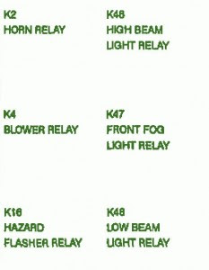
There is also a connection (K2) for a simple signal strength meter. Via resistor R1 and decoupling capacitor C9, pin 9 supplies a DC voltage which is a measure of the received signal strength. At 170 μA the output current is too small to drive an LED, but you could connect an ‘oldfashioned’ moving coil meter. For the antenna you can use a simple wire antenna of about 75 cm long, which is soldered directly to the PCB.

FM Receiver Printed Circuit Board

SMD parts are used everywhere to keep the dimensions as small as possible. Soldering these small parts requires a bit of practice however. The dimensions of this tiny PCB are only 3.2 × 2.7 cm! The circuit contains no difficult coils, only the VCO requires an air-cored inductor with only 4 turns.


This receiver is a mono implementation, but at the output (as already mentioned) the entire multiplexed signal (up to 53 kHz) is available. By using a PLL stereo decoder, such as the TDA7040T, a stereo signal can be generated in a traightforward way from the output signal of the TDA7021T.

FM Receiver Circuit Parts List
Resistors (SMD 0805)
R1 = 8kΩ2
R2 = 10kΩ
R3 = 390Ω
Capacitors (SMD 0805)
C1,C3 = 10nF
C2,C6,C9,C16 = 100nF
C4 = 33pF
C5 = 25pF trimmer (Murata type TZB4Z250AB10R00)
C7,C10 = 1nF5
C8 = 820pF
C11 = 1nF
C12 = 68pF
C13 = 220pF
C14 = 47μF 10V (Nichicon UWX1A470MCL1GB 5.5mmL chip type)
C15 = 3nF3
Inductors
L1 = 36nH (4 turns 0.5mm silver-plated wire, inside diameter 4mm; length 7mm)
L2 = 1μH, SMD case 0805 (fres > 300 MHz)
Semiconductors
IC1 = TDA7021T (SMD in SO16 case)
Miscellaneous
K1,K2 = 2-way pinheader
BT1 = 2-way pinheader + battery holder for 2-4 AA batteries
Read More..

Sunday, September 21, 2014

All about Kenwood car audio

Kenwood products have repeatedly set the benchmark for performance, innovation and reliability for years.

Kenwood products have repeatedly set the benchmark for performance, innovation and reliability for years. Kenwood strives to produce products that will not be obsolete in the near future as well as products that the consumer will be proud to own. Kenwood is also always looking toward the future and keeping its products up-to-date with the latest technology without the consumer having to worry about their entertainment gear being up-to-date. This concept is what Kenwood calls ‘Future Ready/Already’.

Kenwood has always been Future Ready/Already even in the beginnings of the Kenwood Company. The Kenwood Company began by designing and manufacturing Japan’s first FM tuner and solid-state amplifier. After the FM tuner, the company built the most popular stereo receiver ever to sell in the United States. In 1981, Kenwood invented the world’s first audio/video amplifier and audio/video system, many years before other companies would come out with home theater products like them. Kenwood kept the invention streak rolling with the introduction of the first anti-theft car stereo in 1984. All these milestones in Kenwood’s history prove that they are Future Ready/Already.

20 years later, Kenwood is still proving that they are Future Ready/Already by introducing more products, such as the KTC-HR100 HD Radio™ tuner that is the first on the market or the Networked Home Theater Systems that play video and audio files from the home computer. Kenwood also has introduced the 3D MASK Pro™ 3-dimensional control and display system, A.M.S. ™ which is an amplifier management system, Typhoon woofer cones, K-STAT™ self-adjusting power transistors, and Image Enhancer™ tweeter technology. The 2004 Kenwood products bring entertainment of the future for the consumer to enjoy it today.

Staying Future Ready/Already keeps Kenwood examining and refining its products to keep ahead of the competition while pleasing the consumer that has come to depend on Kenwood. All emerging technologies are examined to determine how they can serve the entertainment needs of the consumer. Kenwood diligently searches for more improved ways to make them user friendly, accessible and invisible to the point where the consumer will not even think about the technology itself, the consumer will only know that they are enjoying the product. However, at

Kenwood, Future Ready/Already is more than just features and technologies. Kenwood believes that the future is now and when a consumer owns a Kenwood product, they are ready for tomorrow.

Kenwood offers the best sound and visuals available for the consumer to take on the road either across town or across the nation. The consumer can transform their vehicle into a movie theater, drown out the sound from competition, improve their navigation around town or just simply enjoy the music they enjoy. In addition, with Kenwood’s idea that the future is now, the entertainment gear offered by them is always future ready.

With all the focus that Kenwood puts on their products, they are always ready for yesterday, today and more importantly tomorrow. Kenwood strives to keep there consumers up-to-date which in turn makes for consumers who will become brand loyal to Kenwood.
Read More..

Simple 25W Audio Power Amplifier Circuit

This audio power amplifier project is based on LM1875 amplifier module from National Semiconductor. It can deliver up to 30W of power using an 8 ohm load & dual 30V DC power supplies. It is designed to operate with maximum outside parts with current limit & thermal shutdown protection features . Other features include high gain, quick slew rate, wide power supply range, giant output voltage swing & high current capability.

Summary of the audio amply-fire features:

  • Low distortion: 0.015%, 1 kHz, 20 W
  • Wide power bandwidth: 70 kHz
  • Wide supply range 16V-60V
  • Up to 30 watts output power
  • Internal output protection diodes
  • Protection for AC & DC short diagram to ground
  • 94 dB ripple rejection
  • Plastic power package TO-220
25V Power Supply

The schematic below shows how the +25V DC & -25V DC are obtained. In order to provide power supply for two stereo amplifiers, a power transformer rating of 80VA with 240V/36V middle tapped secondary winding is used. The secondary output of the transformer is rectified by using 1N5401 diodes together with four electrolytic capacitors to smoother the ripple voltage. A fuse & a varistor are connected at the primary input to protect the schema against power surge.


Audio Amplifier Module

The +25V & -25V DC power supply are connected to the audio amplifier module through a 2A fuse with the peripheral devices shown in the schematic below. The audio input signal to be amplified is coupled to pin one of LM1875 through the resistor R1 and electrolytic capacitor E5.

The output signal at pin four of LM1875 can be used to directly drive a 8 ohm loudspeaker. Resistor R6 and capacitor C5 prevent-the capacitance developed at the long speaker leads from driving the amplifier in to High Frequency Oscillation.

A heat-sink with a thermal resistance rating of one.4 Cecilius/Watt or better must be used or else the amplifier module will-be cut-off from operation due to the heat that will build up in the coursework of the operation of the amplifier. Take note that the heat sink tab on the IC module is internally connected to the -25V power supply hence it must be isolated from the heat sink by the use of an insulating washer. If this is not done, the negative rail will be shorted to ground.


Sourced By: Streampowers.blogspot.com
Read More..

High And Low Voltage Cut Off With Time Delay

High And Low Voltage Cut Off With Time Delay The power line fluctuations and cut-offs cause damages to electrical appliances connected to the line. It is more serious in the case of domestic appliances like fridge and air conditioners. If a fridge is operated on low voltage, excessive current flows through the motor, which heats up, and get damaged.

The under/over voltage protection circuit with time delay presented here is a low cost and reliable circuit for protecting such equipments from damages. Whenever the power line is switched on it gets connected to the appliance only after a delay of a fixed time. If there is hi/low fluctuations beyond sets limits the appliance get disconnected. The system tries to connect the power back after the specific time delay, the delay being counted from the time of disconnection. If the power down time (time for which the voltage is beyond limits) is less than the delay time, the power resumes after the delay: If it is equal or more, then the power resumes directly.

This circuit has been designed, built and evaluated by me to use as a protector for my home refrigerator. This is designed around readily available semi-conductor devices such as standard bipolar medium power NPN transistor (D313/SL100/C1061), an 8-pin type 741 op-amp and NE555 timer IC. Its salient feature is that no relay hunting is employed. This draw back is commonly found in the proctors available in the market.

The complete circuit is consisting of various stages. They are: - Dual rail power supply, Reference voltage source, Voltage comparators for hi/low cut offs, Time delay stage and Relay driver stage. Lets now look at the step-by-step design details.

Dual rail power supply.

This is a conventional type of power supply as shown in Figure 1. The power is applied through the step-down transformer (230/12-0-12V/500mA). The DC proportional to the charging input voltage is obtained from bridge rectifier. Two electrolytics are there to bypass any spikes present. Bridge is capable of handling currents up to 1 Amp.

Output is given by: -

V(out) = 0.71 X V (secondary)

= 0.71 X 24V

= 17.04 V

(This equation is similar for the negative rail as well)

Circuit diagram

Low voltage cut off op-amp

Figure 2 shows the use of very common and easily available op-amp 741 as a comparator. The op-amp is available in TO-5 and DIP type packing.

Circuit diagram

In this ckt the zener diode D1 and it’s associated resistor R1 are connected to the non-inverting terminal (+ve) of 741 to give the suitable reference voltage. The DC voltage from the sensor is given to the inverting (-ve) terminal through pre-set R2.This is used to set the input level.

When the sensor input is less than Zener voltage the output from the Op-amp remains high and when it is greater than Zener voltage the output goes low. When the sensing voltage is equal to Zener voltage the output of the op-amp is approximately zero.

This phenomenon is used as a decision for switching the relay and to give cutoff in a low voltage situation.

High voltage cut off op-amp

Here the op-amp is used as a inverted amplifier. See Figure 3.Zener and resistor network gives reference voltage to the inverting terminal (-ve) of op-amp. Sensing voltage derived through the 10 K pre-set is given to the non- inverting (+ve) terminal and this sets the high level cut.

When the input DC from the sensor is less than Zener voltage the output of the op-amp is low and vice-versa. When the input DC voltage is equal to the zener voltage, the op-amps output is approximately zero.

Circuit diagram

Time delay

I’ve selected the 555 timer due to following reasons.

1. Timing from microseconds through hours.

2. Ability to operate from wide range of supply voltages.

3. High temperature stability.

4. Easily Available.

5. Its triggering circuit is quite sensitive.

This is basically a monostable. The external timing capacitor C2 is held initially discharged by the timer. The circuit triggers upon receiving a pulse to its pin 2 when the level reaches 1/3 Vcc. Once triggered., the circuit will remain in that state until the set time is elapsed or power to the circuit cuts off. The delayed period in seconds is 1.1 C2.R1 where R1 is in megohms and C2 is in microfarads. In practice, R1 should not exceed 20 M. If you use an electrolytic capacitor for C2, select a unit for low leakage. The time delay may have to be adjusted by varying R1 to compensate for the wide tolerance of electrolytics.


Circuit diagram

Relay Driver

The output from the voltage level detectors cannot directly drive the relay and hence the relay driver is used.

Circuit diagram

In this a relay (12V <500 ohms) is connected to the collector of npn transistor. the out put voltage from the comparator is applied to the base of npn transistor through a resistance r1. when the output from the comparator is low the transistor is in off state and the relay is in de-energized state. similarly when the output from the comparator goes high the transistor switches on and the flow of current from the collector to emitter of transistor energizes the relay.

Generally in a relay driver circuit, parallel to the relay coil, a diode or a capacitor is used. This is to eliminate the back e.m.f generated by the relay coil when currents are suddenly broken. Capacitor C1 is connected in parallel to the coil, which filters out the back emf but it, slows down the working of relay.

A better method is to connect two diodes (as shown in the figure 5) that stop the relay – transistor junction swinging more than 600mV above the positive rail or below the zero-volt rail. During normal operation the diodes are reverse biased and have no effect on the performance of circuit. But when back emf is induced, the diodes conduct heavily and absorb all transient voltages. However, I have employed the both methods.

The Complete Circuit

Circuit diagram

Under normal operating conditions i.e. when the input voltage is between maximum and minimum limit the output from the both the comparators are low. The transistor Q1 is OFF and the relay is in de-energized (pole connected to N/C pin) state and the output is obtained.

When the input voltage is below or above the limits set by the pre-sets R8 or R9, the output of the Op-Amps goes either low or high and diodes D1 or D2 would be forward biased depending on the situation. Transistor Q1 switches ON and the flow of current from collector to emitter energizes the relay and the output is cutoff.

A small amount of hystersis has been added via feed back resistors R10 & R11 so that the relay turns on when the level falls to a particular value but does not turn again until it raises a substantial amount above this value. Other wise the relay contacts will frequently turn on/off and produce chattering.

Construction Hints

1) I used a piece of varoboard, which has copper strips on one side to mount the components, and housed the entire circuit and the transformer in a discarded ATX PC power supply box.

2) An autotransformer has been used to set the limits. Set the output of the autotransformer to 250V AC and connect it to the primary of transformer T1 (see Figure 1). Then adjust the pre-set R9 such that relay just energizes. This is the high limit. Next set the output of the autotransformer to 200V AC and adjust the pre-set R8 such that the relay energizes. Please note that these are my preferred limits but you may select any range from say 170 to 270V AC.

3) A neon with a suitable resistor could be connected between the AC supply lines as an ON indicator. Alternatively, LED with a current limiting resistor could be connected between the relay coil so when the relay is energized LED will indicate the situation. 

Read More..

The evolution of Google TV based on Android completely L

The

We already knew Google TV, the company system to reach televisions and decoders of our homes. However, the system never made ​​it to be very successful, mainly due to her lack of interest from developers who did not take many applications to this platform. Now, Google announced at its Google I / O 2014 the evolution of the system and now called Android TV.

Unlike Google TV, Android TV would be complemented based on pure Android code L, the new version of the mobile operating system of the company. This would allow developers to easily modify their applications to work directly on this platform, like Android-L (cell phone and tablet) and Android Wear, and not having the need of having to create an entirely new application for this new TV platform.

Currently, a number of applications found on Android and work on the big Lcd TV featuring Android, such as music, games, movies, and more. It is precisely in the area where Android TV game also differs from its predecessor Google TV. Android TV also has a focus on video games, allowing a system is not only television, but also functions as a mini console.

Android TV can be controlled through an Android phone or tablet with L, like a television remote control or video games. In fact, manufacturers are the ones who decide how to offer it in the beginning, is control video game control specially designed for Android TV or regular monitoring of television and users can can choose to use their phones or tablets at any time.

Overall, Android TV interface is very graphical and easy. It works very smoothly and shows you on the home Lcd content recommendations can like, given your history seen or used content, like video games and apps.

Each application has a similar structure where you find a hidden phenomenon on the left side and the other on the right information. The start menu displayed when you open the application and then closes when you enter the information tine each of those categories or play any kind of content.

It has been said that unlike Android mobile phones, Google would control interface and thus offer TV Android experience to users. Thus, manufacturers may not make major changes to the design of Android TV, but if you can add your own content. From now on, the SDK is enabled for developers begin to experience the new Google TV platform and modify or create their applications to be compatible with Android TV.
Read More..

Saturday, September 20, 2014

Fuse Box BMW 318i 1995 Diagram

Fuse Box BMW 318i 1995 Diagram - Here are new post for Fuse Box BMW 318i 1995 Diagram.

Fuse Box BMW 318i 1995 Diagram


Fuse
Fuse

Fuse Panel Layout Diagram Parts: hazard flasher relay, low beam light relay, high beam light relay, blower relay, front fog light relay, horn relay.
Read More..

Fuse Box Toyota 1995 Camry 2 2L 5S FE Diagram

Fuse Box Toyota 1995 Camry 2.2L 5S-FE Diagram - Here are new post for Fuse Box Toyota 1995 Camry 2.2L 5S-FE Diagram.

Fuse Box Toyota 1995 Camry 2.2L 5S-FE Diagram


Fuse
Fuse

Fuse Panel Layout Diagram Parts: EFI, horn, hazard light, dome lamp, headlamp, alternator, ecu, short, starter relay, horn relay, headlight control relay, window defogger relay, fan relay.
Read More..

Fuse Box BMW Z4 Coupe 2007 Diagram

Fuse Box BMW Z4 Coupe 2007 Diagram - Here are new post for Fuse Box BMW Z4 Coupe 2007 Diagram.

Fuse Box BMW Z4 Coupe 2007 Diagram


Fuse
Fuse

Fuse Panel Layout Diagram Parts: brake light, side light, turn indicator, hazard warning flasher, cigar lighter, clutch switch, interior and luggage, comp light, lighting circuit, low beam headlight, high beam headlight, airbag, ASC/DSC, CD changer, central locking system,
Read More..

Friday, September 19, 2014

Acoustic Distress Beacon Circuit diagram

An ELT (Emergency Locator Transmitter, also known as a distress beacon) is an emergency radio transmitter that is activated either manually or automatically by a crash sensor to aid the detection and location of aircraft in distress. This acoustic ELT project is intended for radio control (RC) model aircraft, which every now and then decide to go their own way and disappear into the undergrowth.

Circuit diagram :
Acoustic
Acoustic Distress Beacon Circuit Diagram

The audio locating device described here enables model aircraft that have landed ‘off limits’ to be found again and employs its own independent power supply. The small cam-era battery shown in the schema activates an acoustic sounder when radio contact is lost and produces a short signal tone (bleep) every ten seconds for more than 25 hours. Current consumption in standby and passive (with jumper J1 set) modes is negligible. The timing generator for the alarm tone is the Schmitt trigger AND-gate IC1.B; its asymmetric duty cycle drives a 5 V DC sounder via MOSFET transistor T1. All the time that the RC receiver output is delivering positive pulses, the oscillator is blocked by IC1.A and diode D1. Setting jumper J1 parallel to C2 also disables the oscillator and serves to ‘disarm’ the distress beacon. 


streampowers
Read More..

Automatic TV Lighting Switch

The author is the happy owner of a television set with built-in Ambilight lighting in the living room. Unfortunately, the television set in  the bedroom lacks this feature. To make up for this, the author attached a small lamp to the wall to provide background lighting, This makes  watching television a good deal more enjoyable, but it ’s  not the ideal solution. Although the TV set can be  switched off with the remote  control, you still have to get out of bed to switch off the lamp.

Circuit diagram :
Automatic

Automatic TV Lighting Switch Circuit Diagram

Consequently, the author devised this automatic lighting switch that switches the background light on and off along with the T V set. The entire schema is fitted in series with the mains cable of the TV set, so there’s no need to tinker with the set. It works as follows: R1 senses  the current drawn by the TV  set. It has a maximum value  of 50 mA in standby mode,  rising  to around   500 m A  when  the  set  is  operating. The voltage across R1 is limited by D5 during negative  half- cycles  and  by  D1– D4  during positive half-cycles.  T he  voltage  across  these  four diodes charges capacitor C1 via D6 during positive  half-cycles. This voltage drives the internal LED of solid-state switch TRI1 via R2, which causes the internal triac to conduct and pass the mains voltage to the lamp.   Diode D7 is not absolutely necessary, but  it is recommended because the LED in the  solid-state switch is not especially robust  and cannot handle reverse polarisation. Fuse  F1 protects the solid-state switch against  overloads. T he  value  of  use d  here  (10 Ω)  for  resistor R1 works nicely with an 82-cm (32 inch)  LCD Lcd.

With smaller sets having lower  power consumption, the value of R1 can be  increased to 22 or 33 Ω, in which case you  should use a 3-watt type. Avoid using an  excessively high resistance, as otherwise TRI1 will switch on when the TV set is in standby mode.  Some TV sets have a half-wave rectifier in the  power supply, which places an unbalanced  load on the AC power outlet. If the set only  draws current on negative half-cycles, the cir-cuit won’t work properly. In countries with  reversible AC power plugs you can correct  the problem by simply reversing the plug. Compared with normal triacs, optically cou-pled solid-state relays have poor resistance  to high switch-on currents (inrush currents).

For this reason, you should be careful with  older-model TV sets with picture tubes (due  to demagnetisation diagram). If the relay fails,  it usually fails shorted, with the result that the TV background light remains on all the time. If you build this schema on a piece of perf-board, you must remove all the copper next  to conductors and components carrying  mains voltage. Use PCB terminal blocks with a spacing of 7.5 mm. This way the separation between the connections on the solder  side will also be 3 mm. If you fit the entire  arrangement as a Class II device, all parts of  the schema at mains potential must have a  separation of at least 6 mm from any metal  enclosure or electrically conductive exterior  parts that can be touched.

http://streampowers.blogspot.com/2012/06/automatic-tv-lighting-switch_11.html 
Read More..

Fuse Box Ford 2002 Excursion Junction Diagram

Fuse Box Ford 2002 Excursion Junction Diagram - Here are new post for Fuse Box Ford 2002 Excursion Junction Diagram.

Fuse Box Ford 2002 Excursion Junction Diagram


Fuse
Fuse

Fuse Panel Layout Diagram Parts: drive side front, headlamp circuit, A/C clutch relay, high beam, flash to pass, trailer tow relay, parking lamp, brake pedal position switch, heated oxygen sensor, powertrain control module, air flow sensor, A/C clutch relay, A/C clutch solenoid, radio, cigar lighter, data link connector, seat adjust switch, indicator flasher relay, vehicle security module, vapor management, air suspension, brake pressure switch, ABS control module, restrain control module, reversing lamp, power mirror, injector driver module, fuel injectors, powertrain control module, rear seat entertainment, exterior lamp, driver seat module, DVD player, adjustable pedal, power point, instrument panel, turn signal relay, headlamp.
Read More..

Fuse Box BMW Z4 Coupe Under The Right Side 2007 Diagram

Fuse Box BMW Z4 Coupe Under The Right Side 2007 Diagram - Here are new post for Fuse Box BMW Z4 Coupe Under The Right Side 2007 Diagram.

Fuse Box BMW Z4 Coupe Under The Right Side 2007 Diagram


Fuse
Fuse

Fuse Panel Layout Diagram Parts: low beam headlight, brake light, side light interior indicator, airbag, cd player, central locking system, cigar lighter, interior and luggage, comp lights, lighting circuit.
Read More..

Thursday, September 18, 2014

140W audio amplifier with IC STK070

By using the above amplifier circuit you can hear the sound quality is quite good by a high output power. Maximum voltage circuit pa approximately 55Volt DC. 70-140W output power with impedance 8Ohm.
power
Read More..

Fuse Box Ford 1994 1998 Mustang Battery Junction Diagram

Fuse Box Ford 1994-1998 Mustang Battery Junction Diagram - Here are new post for Fuse Box Ford 1994-1998 Mustang Battery Junction Diagram.

Fuse Box Ford 1994-1998 Mustang Battery Junction Diagram


Fuse
Fuse

Fuse Panel Layout Diagram Parts: constant control relay, main light switch, multifunction switch, starter motor relay, instrument cluster, ABS module, instrument panel, reversing lamp, speed control, daytime running light, ABS module, auxiliary power point, main light switch, rear window defrost, power door lock, CD player, horn, power seat switch, generator, constant control relay, intake manifold relay module.
Read More..

Mercedes Explanation Fuse Box Year Benz 87 420sel Diagram

Fuse Box Mercedes Benz 87 420sel Diagram - Below is Fuse Box Mercedes Benz 87 420sel Diagram.

Fuse Box Mercedes Benz 87 420sel Diagram


Fuse
Fuse

Fuse Panel Layout Diagram Parts: power seat relay, power window relay, auxiliary fuse holder, right speed relay, low speed relay, air pump clutch, air injection, exterior lamp, failure monitoring unit, combination relay, hazard lamp wiper, washer, headlamp washer relay, wiper/washer, power seat diode.
Read More..

Fuse Box BMW 733i 1982 Power Distribution Diagram

Fuse Box BMW 733i 1982 Power Distribution Diagram - Here are new post for Fuse Box BMW 733i 1982 Power Distribution Diagram.

Fuse Box BMW 733i 1982 Power Distribution Diagram


Fuse
Fuse

Radio/Power Antenna, Radio/Power Antenna, Stoplights/Cruise Control, Warning Indicators, Rear Defogger/Sunroof, Automatic Heated Air Conditioner, Interior Lights, Lights: Turn/Hazard Warning, On Board Computer, Auxiliary Fan, Vacuum Pump, Power Window Circuit Breaker, Power Windows, Radio, Auxiliary Fan, Trunk Light, Active Check Control, Dash Lights, Gauges, Idle Speed Control, Interior Lights, Power Mirros, Power Windows, Seatbelt Warning, Speedometer, Warning Indicators, Dash Lights, Lights : Front Park/Tail/Underhood, Lights : Rear Marker/License, Backup Lights/Transmission Range, Lights, Brake Lining Warning, Cruise Control, Fuel Delivery/Evaporative Control, Idle Speed Control, Headlights, Cigar Lighters, Active Check Control, Auto Charging Flaslight., Central Locking, Gauges, Glove Box Light, Heated Door Lock, Ignition Key Warning/Seatbelt Warning, Active Check Control, Front Park/Tail, Active Check Control, Horns, Lights:Turn/Hazard Warning, Wiper/Washer, Active Check Control,
Read More..

Wednesday, September 17, 2014

Fuse Box BMW E46 2005 Diagram

Fuse Box BMW E46 2005 Diagram - Here are new post for Fuse Box BMW E46 2005 Diagram.

Fuse Box BMW E46 2005 Diagram


Fuse
Fuse

Fuse Panel Layout Diagram Parts: outside mirror, parking aid, passenger comp, trunk lighting, radion, rain sensor, rear wiper, reversing light, roller sun bird, secondary air pump, telephone, trailer coupling, tyre pressure, water valve, sinside mirror electrochomic, interior light, light module, make up mirror light, hifting gate illumination, side airbag, sunroof, socket, speed control, sequential transmission, starter interlock, manual soft, navigation, on board computer, diagnose II, monitor, window lift, windscreen washer.
Read More..

Fuse Box Diagram Of 2009 Ford Explorer

Fuse Box Diagram Of 2009 Ford Explorer
The following circuit shows about Fuse Box Diagram Of 2009 Ford Explorer. The parts fuse panel consist of: Fog Lamp, Horn Cigar Lighter, Warning Indicator Lamps, Speed Control Module, Day Night Illumination Relay, Low Oil Warning Relay, Engine Idle Track Relay, Level Indicator, Tail Lamp, Parking Lamp, License Lamps, Turn Signal Lamps, Back Up Lamps, Dual Timer Buzzer, Tachometer, Key Warning Buzzer, Power, Hazard Warning Lamps, Speed Control, Fluids Module, A/C Clutch, Low Fuel Module, Stop lamps, Interval Wiper, Heater Blower Motor, Flash-to-Pass, Ash Receptacle Lamps, Fluid Module, Windshield Wiper, Windshield Washer Pump, Mirror, Climate Control, Power Windows 15 Amps Fuse.
Read More..

Mercedes Explanation Fuse Box Year Benz 2005 C350 Diagram

Fuse Box Mercedes-Benz 2005 C350 Diagram - Below is Fuse Box Mercedes-Benz 2005 C350 Diagram.

Fuse Box Mercedes-Benz 2005 C350 Diagram


Fuse
Fuse

Fuse Panel Layout Diagram Parts: exterior lamp, combination relay, hazard lamp, wiper washer, high speed relay, low speed relay, air pump clutch, headlamp washer, wiper washer, power seat diode, power seat relay, power window relay, auxiliary fuse holder.
Read More..

Tuesday, September 16, 2014

AM Modulator and 50W RF Output Stage

The circuit presented here makes amplitude modulation possible, and it also has the significant advantage that it replaces the somewhat exotic and quite expensive OP603AP output opamp with a standard type. Of course, this amplitude modulator can also be used with other models of function generator or for other purposes. As you know, the gain of an NE592 video opamp can be set to 400, 100 or 10 by means of an external jumper. Intermediate settings can be achieved by using a suitable resistance in place of the jumper. This adjustment takes place in the emitter leads of the differential amplifier, directly at the input to the opamp, where the signal amplitude is low.

AM
A BF245B FET is used here as a controllable resistance. With suitably low signal levels, it provides at least 50% of clean amplitude modulation for modulating signals (LF) up to 10 kHz and modulated signals (HF) up to 20 MHz. The FET can also be driven with a DC voltage to control the amplitude of the output signal over a 10:1 range with low distortion. Any slight asymmetry of the modulated signal can be corrected by applying a small correction voltage via P1. P2 is used to bias the FET at around –2.5 V. The output stage is built using discrete transistors and guarantees a 50 Ω output impedance with low DC offset.

The complete circuit can deliver a constant amplitude output signal of up to 2.5 Vpp (unmodulated) for frequencies ranging to over 20 MHz. If the signal is not modulated, the maximum amplitude can be increased somewhat. Output level controls (a potentiometer and/or range switches), if used, should be placed between the NE592 output and the input of the output stage. In such cases, an emitter-follower stage with a high input impedance might be a good idea, since the opamp should operated with a load of at least 1kΩ. Conceivably, the gate of the FET could be driven via an additional opamp, together with the demodulated signal from the output of the NE592 applied as negative feedback, to achieve higher modulation levels.
Read More..

Explanation Fuse Box Chevy Aveo Instrument Panel 2010 Diagram

Fuse Box Chevy Aveo Instrument Panel 2010 Diagram - This show you about Fuse Box Chevy Aveo Instrument Panel 2010 Diagram.

Fuse Box Chevy Aveo Instrument Panel 2010 Diagram


Fuse
Fuse

Fuse Panel Layout Diagram Parts: Audio, Clock, Immobilizer, A/C Switch, Clock, Power Mirror Unit, Audio, Anti-Theft Module, TPMS, PNP Switch, Reverse Lamp Switch, Cigar Lighter, Brake Switch, TPMS, Anti-Theft Module, Power Mirror Unit, A/C Switch, Rear Defog, Door Lock, Mirror Control Switch, Room Lamp, A/C Switch, Engine Room Fuse Block, TCM, VSS, Fuel Pump, Stoplamp Switch, Horn, DLC, Immobilizer, Trunk Room Lamp, Trunk Open Switch, IPC, Room Lamp, Sensing and Diagnostic Module, Power Jack, Brake Switch, Sunroof Module, Hazard Switch, Wiper Switch, Wiper Motor.
Read More..

Simple Low Power Car Stereo Amplifier

A simple low power car stereo amplifier circuit based on TDA 2003 is shown here. The circuit uses cheap, readily available components and it is very easy to construct. TDA2003 is an integrated car radio amplifier from ST Micro electronics that has a lot of good features like short circuit protection for all pins, thermal over range low harmonic distortion, low cross over distortion etc. 

Circuit diagram :

 A simple low power car stereo amplifier Circuit Diagram


In the circuit given here each TDA2003 is wired as a mono amplifier operating from a 12V supply. Resistors R2 and R3 forms a feedback network that sets the amplifiers gain. C7 is the input DC de-coupling capacitor and C5 couples the speaker to the amplifiers output. C4 is used for improving the ripple rejection while C1 and C2 are employed for power supply filtering. C3 and R1 are used for setting the upper frequency cut-off. Network comprising of C6 and R4 is used for frequency stabilization and to prevent oscillation.

Notes.

  • Assemble the circuit on a good quality PCB.
  • Heat sinks are necessary for both ICs.
  • The circuit can be operated from 12V DC.
  • S1 is the ON/OFF switch

Read More..

Monday, September 15, 2014

10W CAR RADIO AUDIO AMPLIFIER

DESCRIPTION:

The TDA 2003 hasimproved performancewith the same pin configuration as the TDA 2002. The additional features of TDA 2002, very low numberof externalcomponents,ease of assembly, space and cost saving, are maintained. Thedeviceprovidesa high outputcurrentcapability (up to 3.5A) very low harmonic and cross-over distortion. Completely safe operation is guaranteed due to protectionagainst DCand ACshort circuit between all pins and ground,thermal over-range,load dump voltage surge up to 40V and fortuitous open ground.

Circuit diagram:
Circuit diagram 10W CAR RADIO AUDIO AMPLIFIER


Read More..

5V 10A output switching power supply

The Schematic above shows a 10A power suplly with a 5V output and with power 50W. It is a flyback converter operating in the continuous mode. The circuit features a primary side and secondary side controller with full protection from fault conditions such as overcurrent. After the fault condition has been removed the power supply will enter the soft start cycle before recomming normal operation.
10A
Component Values :
Resistor
R1_____100Ω
R2_____1Ω 1W
R3_____10Ω
R4_____100KΩ
R5_____0.33Ω 1W
R6_____10KΩ
R7_____390Ω
R8_____22KΩ
R9_____68Ω
R10____10Ω
R11____3.3Ω
RL_____5Ω 10W

Capacitor
C1_____0.022uF 400V
C2_____470uF  250V
C3_____470uF
C4_____220pF
C5_____470pF
C6_____2200pF
C7_____270pF
C8_____39pF
C9_____11,000uF
C10____10uF
C11____0.047uF


Diode
D1____1N4937
D2____MBR1035
M1____Diode Bridge

Inductor , Transformator
L1_____25uH
T1_____Lp - 9 mH = 1 : 15
T2_____50 uH. n = 1: 3

Transistor
Q1____BUZ80A
Q2____GE IRF823
Read More..