Showing posts with label supply. Show all posts

Thursday, December 11, 2014

Car Laptop Power Supply Adaptor

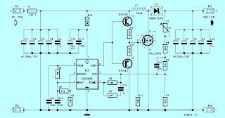
laptop-adaptor-schematic
The laptop adaptor described here plugs into a car cigarette lighter socket and produces a 19V nominal output voltage adjustable by + - 0.5V. The input voltage range is from 9.2V to 15V and the output voltage shows good regulation even with large fluctuations of the input voltage. 
Read More..

Wednesday, November 12, 2014

Adjustment power supply values 1 25 15V Max current 0 5 amp

This is power supply that have Voltage output fine the value has 1.25-15V. From by Output current that be valuable about 0.5 amp that 12V and 0.2 amp that 15V.
When Volt , from 220V houses reach transformer. It will modify Volt 220V to be 18VAC already to change rectifier circuit. Which D1, D2, C1 and R1 wasp be Full wave rectifier circuit. For modify DCV to ACV to a signal DCV. It make get a signal DCV that have voltage at pin 3 of IC1 be 20V. From that time DCV signal this reach fight DC Regulator circuit. Which use IC number LM317. This circuit will perform to maintain one’s position Voltage smoothly. Which level output voltage at get this will go out the way pin 2 of IC1. By have capacitors C2 be voltage filter in order that voltage output level of the circuit is will high class modify to follow fining. The performing fee withstands VR1 there.

Read More..

Friday, November 7, 2014

9 Volt Power Supply Circuit Diagram Using IC 7809

Description
Circuit showing a 9 volt power supply . Here we have used a bridge rectifier and 7809 ic for making this circuit.Where the ic regulate the output to 9 v,1 A .This voltage every time constant.Are you interested ?

Circuit diagram with Parts list.  


Notes. 
  • If a current of 300 mA or above is required, fit a proper heat sink to the IC 7809.
  • If 1A bridge is not available, make one using four 1N 4007 diodes.
Read More..

Simple Gratis Symmetrical Opamp Supply Voltages

Many ways to obtain a set of symmetrical supply voltages for operational amplifiers and comparators from a single +5-V sup-ply voltage have been described already. The simplest option (including with regard to component availability and price) is to use a MAX232, which is available in the 16-pin DIP package for less than 30 p (50 eurocents).

In nearly all microcontroller circuits with an RS232 port, this IC is already present any-way to provide level conversion between TTl signals (5 V) and RS232 signals (nominally ±12 V), so you can obtain a set of symmetric supply voltages for opamps almost free of charge.


It ’s not even necessary to add any circuitry around the IC. Figure 1 shows how a MAX232 is typically wired in a microcontroller circuit.The symmetrical voltages (at around ±9 V) generated from the +5-V supply voltage can be taken from pin 2 (V DD; +9 V) and pin 6 (VEE, –9 V) of the IC.

As you can see from Figure 2, the no-load voltage is nearly 10 V and you can draw up to 5 mA at 9 V, which is enough for most standard opamps and plenty for low-power opamps.
The MAX232 has two charge pumps, each of which has two external capacitors for voltage doubling. These are 10-µF electrolytic capacitors in Figure 1, which yields a somewhat stabler output voltage than the standard circuit with 1 µF as shown in Figure 2. The charge pumps of the MAX232 are operated at an oscillator frequency of around 50 kHz, so the amount of ripple on the output voltage is quite small (typically less than 10 mV with a 2-mA load).


This means that in most cases you can manage without any additional filtering of the output voltage. In sensitive applica-tions, such as amplification of small audio or measurement signals by one or more opamps, it’s a good ideal to use a small gyrator circuit for additional suppression of the residual 50-kHz signal. Figure 3 is an example of such a circuit that has been proven frequently in practice. Of course, you can use other types of complimentary small-signal silicon transistors, such as the BC547 (NPN) and BC577 (PNP), in place of the BC550 (NPN) and BC560 (PNP) shown on the schematic.

Transistors in the current gain class ‘B’ (such as the BC547B and BC557B) are also suitable, and the values of the capacitors between the bases of the transistors and ground can also be increased (e.g. 100 µF) or decreased (e.g. 1 µF).  
Read More..

Thursday, October 30, 2014

AC Power Amplifier with Simplified Power supply

AC
Figure 18b. DC Equivalent of circuit 18a.

Figure 18a shows an AC amplifier that works with a single power supply. In this amplifier the load RL, and the signal source are connected directly to the earth and not with the VBias voltage.

Therefore, the voltage applied to the input (VP) of the operational amplifier is equal to the voltage bias (VBias). The voltage in the reverse input VN, is equal to:

VN = VD + VP

And since in an ideal operational amplifier, VD = 0, we have:

VN = VP

Therefore, both inputs of the operational amplifier having the same voltage (equal to VBias). The input capacitor (Cin) blocks the flow of direct current through the resistor R1.

Therefore, on the direct current circuit of Figure 18 is equivalent to the circuit shown in Figure 18b, which is a voltage follower with voltage gain equal to the unit (AV = 1). Therefore, the constant voltage applied to the input is equal to VBias and the voltage at the output is equal to:

V0 = AV x VBias = 1xVBias

Therefore, the two inputs and the output of the operational amplifier have the same voltage (VBias). If VBias = VCC / 2, then the inputs and the output are located between +Vcc and ground (0 volts), and therefore the amplifier allows the positive and the negative change at the output signal. The output voltage of the amplifier can be determined as follows: The current I1 flowing through the resistor R1 and the capacitor CIN is equal to the current I2 flowing through resistor R, so we say:

I1 = I2

The current flowing through R1 is equal to the voltage difference between the combination of the range R1 and CIN, ie we have:


Where VA = VIN,
VB = VP = VD + VBias = VBias (because VD = 0)

Also:


So:


The current I2 is equal to


Since I1 = I2 we have:


From the above equation we get:


By multiplying both sides with R2 we have:


Figure. 19

Note that the expression in the first part in brackets of equation 2, represents the voltage gain of an amplifier to correct AC wiring, and the second part in brackets represents the second voltage gain of an amplifier in reverse AC wiring. Substituting the value of Z1 in the above equation we get:


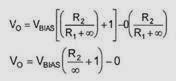
At rest, VIN = 0V, and since the impedance of a capacitor (capacitance Xc = 1/2pfC) to direct current (f = 0Hz) is essentially infinite, the output voltage is:

http://saaqibs.blogspot.com/2014/02/ac-power-amplifier-with-simplified.html


Because R2 / infinity = 0
We have:
V0 = VBias(0 + 1) = VBias
Vo = VBias

From the above equation we see that the output voltage is equal to the polarization voltage (VBias). Therefore, the voltage at both inputs and the voltage output of the operational amplifier are equal. Due to the presence of the input capacitor, the voltage gain of the amplifier AC now depends on the frequency of the signal applied to the input of the amplifier. The capacitor CIN input and resistor R1 form a high pass RC filter. The values R1 and CIN determine the low cut-off frequency of the amplifier. The frequency at which the voltage gain is decreased by -3dB, is the low cut-off frequency, and can be determined using the following equation:


For example, if CIN = 1pF and R1 = 10Kohm, then the low frequency cutoff is 15.9Hz. Signals having lower frequency than the cutoff frequency, are reduced by 20 decibels (20 decibels per decade) for each tenfold reduction in frequency (one decade corresponds to a ten-fold increase or decrease in frequency). If a capacitor is connected in series with the output, the capacitor will prevent the DC current and will only allow the AC signal to pass, and thus the bias voltage to the load by changing the voltage VBias of the earth (0 volts). The capacitor output together with the load RL forms a low pass RC filter which causes attenuation at low frequencies. Note that although the circuit shown in Figure 16 uses the smallest number of components, may be unsuitable in certain applications where the signal source, the load, and the proper input of the operational amplifier, it must be connected to a bias voltage in such cases should use the circuit shown in Figure 18. Notice that the voltage gain in the circuit shown in Figure 18 depends on agreements frequencies, due to the presence of the input capacitor. You may think that the circuit shown in Figure 18 will work correctly if removing the input capacitor CIN (Fig. 19), but, this capacitor must remain otherwise the circuit will not work correctly. The output voltage of the amplifier in Figure 19 is given by the following equation:


The above equation can be proved very simply by using the principle of ultra-rustling, as follows: First we set VBias = 0, the amplifier is now essentially an inverse amplifier and the output voltage is given by the following equation:

VO(-) = VIN x (-R2/R1)

Then we set VIN = 0, the amplifier is now essentially a floor depth in amplifier and the output voltage is given by the following equation:

V0(+) = VBias (1 + R2/R1)

The total output voltage of the amplifier is now equal to:
V0 = V0(-) + V0(+), or Observe that The above equation is the same as Equation 2 if you replace Z1 with R1.


Figure 20. AC amplifier.


In the absence of an input signal, the dc voltage at the output will try to become equal with


For example, if R1 = R2 = 10Kohm, Vcc = 10V, and VBias = 5V, then:

V0 = (1 +2) VBias = (3)x(5V) = 15V

However, this is not possible because the maximum positive output voltage can have with this amp is less than +10 V.

Therefore, the output voltage is always less than the positive voltage of the power supply. Therefore, when an input signal applied alternating current, the output remains saturated during the negative half-period of the input signal. The output will also remain saturated just below the positive trend of +10 V of power supply, for the positive input signals. The circuit shown in Figure 20 is a correct AC amplifier that operates with a single power supply. The voltage between the reverse and correct input is substantially equal to zero volts. After VN = VD + VP and VD = 0, the input terminal of the reverse is also VBias = Vcc/2, relative to the earth. Therefore, both inputs of the operational amplifier is at the same voltage (VBias). The output voltage can be determined as follows:

The current I1 flowing through Z1 is equal to the current I2 flowing through resistor R2. The voltage across Z1 is equal to VB-VA, where VB = VBias and VA = 0.

So we have:


The voltage across R2 is equal to:

Vo = VB: therefore


Since I1 = I2, we have:


Again rearranging the above equation we take:


By multiplying both sides with R2 we get:


The impedance Z1 is given by the equation:


At DC (f = 0Hz), the resistance of the capacitor Cin is infinite:


Consequently in DC we get:


and so VO = VBias.

We will now examine the various circuits to generate the dc voltage bias, which is sometimes called virtual ground. Before you choose a circuit output dc voltage bias must specify load regulation, power supply rejection, power dissipation and the output impedance of the circuit bias. The final decision on what bias circuit will be used in an application depends on the cost and the space we have available to us. The simple voltage divider shown in Figure 21, can be used to produce the constant bias voltage (VBias). This circuit has low load regulation. I.e. as the load current increases, the output voltage of this circuit (bias voltage) is reduced. An explanation of the load regulation and line regulation given below.


Figure 21

Figure 21. A simple voltage divider can be used to generate the bias voltage (VBias).


Figure 22

Figure 22(a). Equivalent circuit of an ideal power supply, (b) Equivalent circuit of an actual power supply.


An ideal power supply provides an output voltage that remains constant regardless of the load current, and is also independent of temperature variations, and also from any changes in the supply voltage of the alternating current network. Figure 22A shows the equivalent circuit of an ideal power supply. In the case of a practical power supply, the output voltage decreases as the load current increases. This is why a real power has an equivalent internal resistance, because of the various components of which consists of the power supply circuit. The equivalent circuit of an actual power supply shown in Figure 22b, where VNL is the output voltage with an open circuit (ie the output voltage when there is no load at the output terminals of the power supply), and R1 is the total internal resistance of the power supply. When a load is connected to the output of the power supply, the output voltage, ie the voltage across the load (VL = IL x RL) is less than the output voltage (VNL) with open circuit. This is because the resistors RL, and RI, form a voltage divider and the voltage across the load is given by:


When the load current increases, the voltage drop across the internal resistance RI also increases, and therefore, the output voltage decreases. The reduction of the output voltage as the load current increases, is a disadvantage. The output voltage of a typical power supply compared to the load current is shown in Figure 23. An ideal power supply has an output voltage that is constant regardless of the load that connects to the output terminals. Obviously, if the internal resistance RI is zero or very small compared to the RL, then output voltage VO is constant and equal to the VNL. The change of the DC output voltage of the power supply relative to the continuous load current is called, simply load regulation or regulation.

The regulation is defined as follows:


The load regulation can be expressed as a percentage:


An ideal power supply would have 0 load regulation, since an ideal power supply is:
RI = 0, and therefore VL = VNL.

Example. The open circuit voltage (i.e., when RL = infinity) of a power supply is VNL = 20V, and when a load is connected to terminals of the power supply, the output voltage drops to 15V. The load regulation of the power supply is given by:


Figure. 23


Ie the regulation of the power supply is 25%.
Read More..

Tuesday, October 28, 2014

IC555 Negative supply voltage low current

This circuit is a depressing power supply integrated. Which can be situated useful to circuits with the intention of carry out not need much course. Using IC rejection. 555. The primary of the circuit.

IC555
IC555 Negative supply voltage low current schematic
Exertion of the circuit is IC1, R1, R2 and C1. The range of the A lasting Multi Vibrator, and the output is a open place wave. It is a upbeat hint pulse frequency of 2.3 kHz output pin 3 of IC1.And C3 and D1 connected to circuit CLAMP. to it serves to signal a positive pulse to pulse signal unenthusiastic.The D2 and C3 play-act negative pulse warning sign is converted order current (DCV) electrical signals. The negative power. in this fashion the output voltage to a negative DC electrical.

Read More..

Monday, October 27, 2014

Switch Mode Power Supply

The purpose of these plans is normally straightforward, helped by the first-rate certification with the intention of is free. A average paradigm of a switch-mode power supply is that based on the LM2671 otherwise LM2674. The components intended for it are presented for outputs of 3.3 opposed to, 5 V and 12 V. near is and a version provided that a presettable output voltage. in the specified use, the materials can release currents of up to 500 mA. remark-worthy is the prohibitive switching frequency of 260 kHz.
Switch Mode Power Supply Circuit


pro with the aim of just low-appraise inductor and capacitors are required, and this results hip exceptional efficiency and unimportant dimensions. In typical circumstances, the efficiency is 90% and may perhaps even quit up to 96%. Both ICs provide protection in contradiction of current and heat overloads. The LM2671 has a add up to of other facilities such because soft start and the option to go to work with an outside grandfather clock. The latter enables several materials to happen in time so as to transfer better control of a few EMC (ElectroMagnetic Compatibility). The relevance publicized trendy the diagram provides an output voltage of 5 in oppositin to and an output current of up to 500 mA. Diode D1 is a Schottky type (Uco≥ 45 versus and Imax≥ 3 A).
Read More..

Thursday, October 23, 2014

Adapter power supply and charger circuit

Basically adapter, power supply and charger circuit has a similar construction which consists of a transformer, rectifier (rectifier) and smoothing the voltage. For there is usually an additional power supply voltage stabilizer of voltage regulator IC LM series 78XX or 79XX .
Below is a schematic circuit adapter, power supply, or battery charger (for gadgets, mobile phones, MP4player, smartphone) that is equipped with a 5V voltage stabilizer:

Adapter, power supply and charger circuit

Read More..

Saturday, October 18, 2014

CA3140 TIP41 2N3055 Lab Power Supply 0 30V 2A


This is the schematic of the 30V/2A power supply I use in my own lab.It may look very complex, but it really isn’t very difficult to understand: it uses only the knowledge we’ve learned in the previous lessons.
The top part looks like the power supply we built in Lesson 7: the transformer L1 transforms the outlet voltage to a safe 30V, which is rectified by bridge rectifier G2 and smoothed by capacitor C5. Transistors T3 and T6 form a darlington transistor. This darlington replaces transistor T1 in Lesson 7. However, the base voltage is not controlled by a simple potmeter, but by an ‘electronic potmeter’ with voltage feedback. The advantage of this feedback is a load-independent output voltage.

Read more original source:
http://www.hobby-electronics.info/go.php?to=11000
Read More..

Monday, October 13, 2014

13 8V 40A High current Power Supply


My good Friend want circuit power supply for VR (Radio Sound), I find to this good Website.

more 13.8V power supply

Intro Detail :

SPECIFICATION

· Input voltage: 240

· Output voltage: 13.2V DC

· Output current: 40A DC

· Over current protection: current limiting al 40A

· Short circuit protection: Regulator shut off.

· Over voltage protection: Shuts off DC input and discharges input stage reservoir.

· Over temperature protection: Fan automatically operates as heat sink temperature of 65°C.

· Indicators: Power ON LED and Short circuit Protection active LED.

THIS PROJECT describes a Protected 13.2V 40A Power Supply Unit which, provided the heat sinking and cooling fan are suitable, is capable of running at full power at 100% duty cycle. It features soft starting, over voltage, current limiting, short circuit protection and automatic fan control. It is a substantial project that is not for the novice constructor.

CIRCUIT DESCRIPTION
THE HEAVY CURRENT carrying connections are shown in bold in Fig 1. The mains input passes through an EMC filter, protection fuse F1 and ON/OFF switch S 1 to transformer TI. The secondary output of TI is rectified by D I but cannot pass through open relay contacts RL1a. To start the PSU switch, S2 is operated allowing limited current to pass via R1 to slowly charge the reservoir capacitor C1. As C1 charges, the RL1 a pulls in closing the relay contacts and shorting out R1 and S2 placing the PSU in the ON state.

Voltage regulator IC1 is the popular 723. A 7.2V reference on IC 1:6 is fed to non-inverting ICI:5. This is compared with a sample of the PSU output voltage via RI3, RI4 and R15 to inverting input at ICI:4. The 723 can source 150mA at ICl:10, so transistor TR2 acts as a Darlington driver for the pass transistors TR3 to TR7 inclusive. Resistors R21 to R25 are current sharing resistors and the voltage across them is proportional to the current drawn by the PSU load.

When the current through R21reaches 8A (i.e. a total PSU current output of 40A) the voltage across R11 and R12 is 0.88V and is tapped from R I I to bias a transistor inside IC1 which robs IC1: 10 of some current, forcing the PSU into a current limiting mode.

Read More..

Sunday, October 5, 2014

5 Watt Digital Power Supply


5 Watt Digital Power Supply is a small +5V power supply, which is useful when experimenting with digital electronics. Small inexpensive wall tranformers with variable output voltage are available from any electronics shop and supermarket. Those transformers are easily available, but usually their voltage regulation is very poor, which makes then not very usable for digital circuit experimenter unless a better regulation can be achieved in some way. The following circuit is the answer to the problem.

This circuit can give +5V output at about 150 mA current, but it can be increased to 1 A when good cooling is added to 7805 regulator chip. The circuit has over overload and therminal protection.
Read More..

Latest Student DC Power Supply

Heres a simple DC power supply having three output terminals: regulated +5VDC, unregulated +10VDC and 7.5VAC. The supply is suitable for microcontroller experimenting for any student.


My workbench has many broken devices and most of them will be used as the part for making the electronic projects. One day I looked at the broken radio, I found theres an AC line cord with socket and a transformer. Actually I like the way they used AC socket with the AC cord. I thought why dont make a simple DC supply from these parts. Most of the DC adapters provide only DC output. But not AC output, some of the uC circuit need a +5V for digital circuit, some need an AC line voltage for timing synchronization, digitizing sine wave, and some need unregulated for relay driving. So I designed above circuit for lab usage.

The DC power supply circuit is a linear regulator providing galvanic isolation from main line through the use of isolation transformer. Quite safe for experimenting with AC voltage. Below pictures show the example of input/output terminal connections, labeling and components placement in the box. The circuit can be built using universal PCB. The output terminal is for big load connection so this makes it quite strong and good electrical contact to the load being used.


Simple DC Power Supply for Students
Read More..

Monday, September 15, 2014

5V 10A output switching power supply

The Schematic above shows a 10A power suplly with a 5V output and with power 50W. It is a flyback converter operating in the continuous mode. The circuit features a primary side and secondary side controller with full protection from fault conditions such as overcurrent. After the fault condition has been removed the power supply will enter the soft start cycle before recomming normal operation.
10A
Component Values :
Resistor
R1_____100Ω
R2_____1Ω 1W
R3_____10Ω
R4_____100KΩ
R5_____0.33Ω 1W
R6_____10KΩ
R7_____390Ω
R8_____22KΩ
R9_____68Ω
R10____10Ω
R11____3.3Ω
RL_____5Ω 10W

Capacitor
C1_____0.022uF 400V
C2_____470uF  250V
C3_____470uF
C4_____220pF
C5_____470pF
C6_____2200pF
C7_____270pF
C8_____39pF
C9_____11,000uF
C10____10uF
C11____0.047uF


Diode
D1____1N4937
D2____MBR1035
M1____Diode Bridge

Inductor , Transformator
L1_____25uH
T1_____Lp - 9 mH = 1 : 15
T2_____50 uH. n = 1: 3

Transistor
Q1____BUZ80A
Q2____GE IRF823
Read More..

Simple 2 Watt Small Switching Power Supply Wiring diagram Schematic

In this small switching power supply, a Schmitt trigger oscillator is used to drive a switching transistor that supplies current to a small inductor. Energy is stored in the inductor while the transistor is on, and released into the load schema when the transistor switches off.

2 Watt Small Switching Power Supply Circuit Diagram

Simple

The output voltage is dependent on the load resistance and is limited by a zener diode that stops the oscillator when the voltage reaches about 14 volts. Higher or lower voltages can be obtained by adjusting the voltage divider that feeds the zener diode. The efficiency is about 80% using a high Q inductor.
Read More..

Sunday, September 14, 2014

35 Ampere Power Supply

35
To make 12Volt 35 Amp Power Supply such as those titles can using LM7812 voltage regulator as the regulator 12 Volt DC and as a power supply can use transistor  TIP2955 .

Series Power Supply 12Volt 35 Amp uses 6 units TIP2955 type power regulator transistors. I use a type MJ2955 TIP2955 not because packaging TIP2955 easier to install heatsink. The series 12Volt 35 Amp Power Supply can be loaded up to 35A depending on the travo which we attach. The series 12Volt 35 Amp Power Supply is very simple, because the voltage regulators make use of IC7812 which will leave a power regulator alone. For more details, series 12Volt 35 Amp Power Supply can be seen in thethe following figure .

12Volt
12Volt 35Ampere schematic


If want the maximum currents up to 35A not only reduced the live circuit TIP2955nya power regulator, no need to 6 levels as seen in the image series 35 Ampere Power Supply 12Volt above.
Read More..