Showing posts with label with. Show all posts

Thursday, November 20, 2014

1 Lamp with 2 switches

Series 1 light 2 switch configuration is intended to control lights from two locations arefar apart. Application of series 1 light with 2 switches are often implemented in thehallway or tunnel. In the application in a hallway or tunnel, with a series like this we can turn on or turn off the light from each tunnel or hallway door. The number of lights can bereproduced by paralleling. The circuit is very simple because only built of 1 and 2pieces of fruit lamp selector switch. If you want to use a lamp with a power greater then the switch can be replaced with 1 piece contactor (relay) for each switch. Then switchused to turn on and turn off the relay replacement S1 and S2.

The working principle with 2 series 1 light switch is the light will light when the S1 and S2 different position, and the lights will be on at the time of the switch position S1 and S2 together. In the installation of switches S1 and S2 each put at the end of the hallway or tunnel.
Read More..

Mini Amplifier with 3 Transistor

Mini 3 transistor amplifier is a simple amplifier with 50mW power drawn by 3 transitor.
The series of three mini-amplifier transistors can be used for loud speaker 8 ohm load. Source voltage required to activate the mini-amplifier can be drawn from the batteries 9V.Rangkaian 3 transistor amplifier is often used in simple portabe audio devices such as radios or small tape recorder. Mini-transistor amplifier circuit 3 is quite simple as shown in the figure below.


Mini


Mini-transistor amplifier circuit 3 includes type of amplifier OTL (Output Transformer Less). Mini-transistor amplifier circuit 3 is used for output coupling capacitors. Amplifier circuit is simple and suitable when used for audio amplifier experiment.
Read More..

Wednesday, November 19, 2014

Adjustable Switching Regulator Circuit with LM2576

The Adjustable Switching Regulator Circuit with LM2576 are monolithic integrated circuits that provide all the active functions for a step-down (buck) switching regulator, capable of driving 3A load with excellent line and load regulation. These devices are available in fixed output voltages of 3.3V, 5V, 12V, 15V, and an adjustable output version.
LM2576 IC Package
Requiring a minimum number of external components, these regulators are simple to use and include internal frequency compensation and a fixed-frequency oscillator. The Adjustable Switching Regulator Circuit with LM2576 offers a high-efficiency replacement for popular three-terminal linear regulators. It substantially reduces the size of the heat sink, and in some cases no heat sink is required.


IC Switching Regulator Circuit with LM2576

A standard Adjustable Switching Regulator Circuit with LM2576 of inductors optimized for use with the LM2576 are available from several different manufacturers. This feature greatly simplifies the design of switch-mode power supplies.

Other features include a guaranteed ±4% tolerance on output voltage within specified input voltages and output load conditions, and ±10% on the oscillator frequency. External shutdown is included, featuring 50 μA (typical) standby current. The output switch includes cycle-by-cycle current limiting, as well as thermal shutdown for full protection under fault conditions.

Features Adjustable Switching Regulator Circuit with LM2576 :
- 3.3V, 5V, 12V, 15V, and adjustable output versions
- Adjustable version output voltage range,1.23V to 37V
- Guaranteed 3A output current
- Wide input voltage range, 40V up to 60V for HV version
- Requires only 4 external components
- 52 kHz fixed frequency internal oscillator
- TTL shutdown capability, low power standby mode
- High efficiency
- Uses readily available standard inductors
- Thermal shutdown and current limit protection
- P+ Product Enhancement tested
Read More..

Wednesday, November 12, 2014

RTS0072B Voice changer circuit project with Diagram Circuit

A very simple voice changer electronic circuit project can be designed using the RTS0072B single chip CMOS LSI designed for voice changer, which can transpose or distort one voice into another voice by encoding the input audio signals in normal speed and transmit the output audio signals with unusual speed. That is accomplished by sampling the input audio signals into digital signals and re-arranges the digital signals to generate different voice from the user normal voice.
This circuit project is very simple and require few external electronic parts . Circuit must be powered from a DC power supply circuit that will provide a fixed output voltage between 3 and 5 volts .
This circuit has various voice effects like transposing voice (higher or lower) ,amplifying voice and robot voice .
As you can see in this project is used a 9 volts DC power supply , because this circuit uses a LM386 audio amplifier IC that will amplify the output signal .
Read More..

Tuesday, November 11, 2014

TDA1151 based Motor Speed Controller circuit with explanation

This motor speed controller uses a TDA1151 monolithic integrated circuit , designed by ST Microelectronics . TDA1151 motor speed controller circuit is designed in a SOT-32 plastic package and can be used for small applications where the space inside is very critical .
Also this circuit diagram can be used as speed regulator for DC motors of record players, tape and cassette recorders, movie cameras, toys or other low cost applications.

This speed controller circuit can provide a high output current up to 800 mA without any additional components and has a low quiescent current of 1.7mA .
The TDA1151 require a low reference voltage ( around 1.2 volts ) and it has a excellent parameters stability versus temperature .
The maximum voltage that can be applied to the TDA1151 is around 20 volts .
As you can see in the circuit diagram the TDA1151 require just few common external components and is very easy to design .

Source: electroniq.net

Read More..

Saturday, November 1, 2014

LED BACKLIGHTING SOLUTION WITH LM3430 and LM3432 ELECTRONIC DIAGRAM


LED BACKLIGHTING SOLUTION WITH LM3430 and LM3432 ELECTRONIC DIAGRAM

The LM3432 is a 6-channel high voltage current regulator which provides a simple solution for LED backlighting applicationsand the LM3430 is a companion device to supply high voltage required to drive serially connected LED strings. The LM3430 and the LM3432 provide a complete solution to most HB-WLED backlighting applications for notebook and PC monitor. In this application note, a typical example for a solution to drive six strings of twelve LEDs in series running at 20mA per string is described in details.
Read More..

Thursday, October 30, 2014

AC Power Amplifier with Simplified Power supply

AC
Figure 18b. DC Equivalent of circuit 18a.

Figure 18a shows an AC amplifier that works with a single power supply. In this amplifier the load RL, and the signal source are connected directly to the earth and not with the VBias voltage.

Therefore, the voltage applied to the input (VP) of the operational amplifier is equal to the voltage bias (VBias). The voltage in the reverse input VN, is equal to:

VN = VD + VP

And since in an ideal operational amplifier, VD = 0, we have:

VN = VP

Therefore, both inputs of the operational amplifier having the same voltage (equal to VBias). The input capacitor (Cin) blocks the flow of direct current through the resistor R1.

Therefore, on the direct current circuit of Figure 18 is equivalent to the circuit shown in Figure 18b, which is a voltage follower with voltage gain equal to the unit (AV = 1). Therefore, the constant voltage applied to the input is equal to VBias and the voltage at the output is equal to:

V0 = AV x VBias = 1xVBias

Therefore, the two inputs and the output of the operational amplifier have the same voltage (VBias). If VBias = VCC / 2, then the inputs and the output are located between +Vcc and ground (0 volts), and therefore the amplifier allows the positive and the negative change at the output signal. The output voltage of the amplifier can be determined as follows: The current I1 flowing through the resistor R1 and the capacitor CIN is equal to the current I2 flowing through resistor R, so we say:

I1 = I2

The current flowing through R1 is equal to the voltage difference between the combination of the range R1 and CIN, ie we have:


Where VA = VIN,
VB = VP = VD + VBias = VBias (because VD = 0)

Also:


So:


The current I2 is equal to


Since I1 = I2 we have:


From the above equation we get:


By multiplying both sides with R2 we have:


Figure. 19

Note that the expression in the first part in brackets of equation 2, represents the voltage gain of an amplifier to correct AC wiring, and the second part in brackets represents the second voltage gain of an amplifier in reverse AC wiring. Substituting the value of Z1 in the above equation we get:


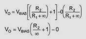
At rest, VIN = 0V, and since the impedance of a capacitor (capacitance Xc = 1/2pfC) to direct current (f = 0Hz) is essentially infinite, the output voltage is:

http://saaqibs.blogspot.com/2014/02/ac-power-amplifier-with-simplified.html


Because R2 / infinity = 0
We have:
V0 = VBias(0 + 1) = VBias
Vo = VBias

From the above equation we see that the output voltage is equal to the polarization voltage (VBias). Therefore, the voltage at both inputs and the voltage output of the operational amplifier are equal. Due to the presence of the input capacitor, the voltage gain of the amplifier AC now depends on the frequency of the signal applied to the input of the amplifier. The capacitor CIN input and resistor R1 form a high pass RC filter. The values R1 and CIN determine the low cut-off frequency of the amplifier. The frequency at which the voltage gain is decreased by -3dB, is the low cut-off frequency, and can be determined using the following equation:


For example, if CIN = 1pF and R1 = 10Kohm, then the low frequency cutoff is 15.9Hz. Signals having lower frequency than the cutoff frequency, are reduced by 20 decibels (20 decibels per decade) for each tenfold reduction in frequency (one decade corresponds to a ten-fold increase or decrease in frequency). If a capacitor is connected in series with the output, the capacitor will prevent the DC current and will only allow the AC signal to pass, and thus the bias voltage to the load by changing the voltage VBias of the earth (0 volts). The capacitor output together with the load RL forms a low pass RC filter which causes attenuation at low frequencies. Note that although the circuit shown in Figure 16 uses the smallest number of components, may be unsuitable in certain applications where the signal source, the load, and the proper input of the operational amplifier, it must be connected to a bias voltage in such cases should use the circuit shown in Figure 18. Notice that the voltage gain in the circuit shown in Figure 18 depends on agreements frequencies, due to the presence of the input capacitor. You may think that the circuit shown in Figure 18 will work correctly if removing the input capacitor CIN (Fig. 19), but, this capacitor must remain otherwise the circuit will not work correctly. The output voltage of the amplifier in Figure 19 is given by the following equation:


The above equation can be proved very simply by using the principle of ultra-rustling, as follows: First we set VBias = 0, the amplifier is now essentially an inverse amplifier and the output voltage is given by the following equation:

VO(-) = VIN x (-R2/R1)

Then we set VIN = 0, the amplifier is now essentially a floor depth in amplifier and the output voltage is given by the following equation:

V0(+) = VBias (1 + R2/R1)

The total output voltage of the amplifier is now equal to:
V0 = V0(-) + V0(+), or Observe that The above equation is the same as Equation 2 if you replace Z1 with R1.


Figure 20. AC amplifier.


In the absence of an input signal, the dc voltage at the output will try to become equal with


For example, if R1 = R2 = 10Kohm, Vcc = 10V, and VBias = 5V, then:

V0 = (1 +2) VBias = (3)x(5V) = 15V

However, this is not possible because the maximum positive output voltage can have with this amp is less than +10 V.

Therefore, the output voltage is always less than the positive voltage of the power supply. Therefore, when an input signal applied alternating current, the output remains saturated during the negative half-period of the input signal. The output will also remain saturated just below the positive trend of +10 V of power supply, for the positive input signals. The circuit shown in Figure 20 is a correct AC amplifier that operates with a single power supply. The voltage between the reverse and correct input is substantially equal to zero volts. After VN = VD + VP and VD = 0, the input terminal of the reverse is also VBias = Vcc/2, relative to the earth. Therefore, both inputs of the operational amplifier is at the same voltage (VBias). The output voltage can be determined as follows:

The current I1 flowing through Z1 is equal to the current I2 flowing through resistor R2. The voltage across Z1 is equal to VB-VA, where VB = VBias and VA = 0.

So we have:


The voltage across R2 is equal to:

Vo = VB: therefore


Since I1 = I2, we have:


Again rearranging the above equation we take:


By multiplying both sides with R2 we get:


The impedance Z1 is given by the equation:


At DC (f = 0Hz), the resistance of the capacitor Cin is infinite:


Consequently in DC we get:


and so VO = VBias.

We will now examine the various circuits to generate the dc voltage bias, which is sometimes called virtual ground. Before you choose a circuit output dc voltage bias must specify load regulation, power supply rejection, power dissipation and the output impedance of the circuit bias. The final decision on what bias circuit will be used in an application depends on the cost and the space we have available to us. The simple voltage divider shown in Figure 21, can be used to produce the constant bias voltage (VBias). This circuit has low load regulation. I.e. as the load current increases, the output voltage of this circuit (bias voltage) is reduced. An explanation of the load regulation and line regulation given below.


Figure 21

Figure 21. A simple voltage divider can be used to generate the bias voltage (VBias).


Figure 22

Figure 22(a). Equivalent circuit of an ideal power supply, (b) Equivalent circuit of an actual power supply.


An ideal power supply provides an output voltage that remains constant regardless of the load current, and is also independent of temperature variations, and also from any changes in the supply voltage of the alternating current network. Figure 22A shows the equivalent circuit of an ideal power supply. In the case of a practical power supply, the output voltage decreases as the load current increases. This is why a real power has an equivalent internal resistance, because of the various components of which consists of the power supply circuit. The equivalent circuit of an actual power supply shown in Figure 22b, where VNL is the output voltage with an open circuit (ie the output voltage when there is no load at the output terminals of the power supply), and R1 is the total internal resistance of the power supply. When a load is connected to the output of the power supply, the output voltage, ie the voltage across the load (VL = IL x RL) is less than the output voltage (VNL) with open circuit. This is because the resistors RL, and RI, form a voltage divider and the voltage across the load is given by:


When the load current increases, the voltage drop across the internal resistance RI also increases, and therefore, the output voltage decreases. The reduction of the output voltage as the load current increases, is a disadvantage. The output voltage of a typical power supply compared to the load current is shown in Figure 23. An ideal power supply has an output voltage that is constant regardless of the load that connects to the output terminals. Obviously, if the internal resistance RI is zero or very small compared to the RL, then output voltage VO is constant and equal to the VNL. The change of the DC output voltage of the power supply relative to the continuous load current is called, simply load regulation or regulation.

The regulation is defined as follows:


The load regulation can be expressed as a percentage:


An ideal power supply would have 0 load regulation, since an ideal power supply is:
RI = 0, and therefore VL = VNL.

Example. The open circuit voltage (i.e., when RL = infinity) of a power supply is VNL = 20V, and when a load is connected to terminals of the power supply, the output voltage drops to 15V. The load regulation of the power supply is given by:


Figure. 23


Ie the regulation of the power supply is 25%.
Read More..

Wednesday, October 29, 2014

Light Gate with Counter Circuit Diagram

The circuit described here counts the number of times that an infrared beam is interrupted. It could be used to count the number of people entering a room, for instance, or how often a ball or another object passes through an opening (handy for playing shuffleboard). The heart of the circuit consists of you guessed it a light gate! Diode D1 is an IR diode that normally illuminates IR transistor T1. The light falling on T1 causes it to conduct to a certain extent. The resulting voltage on the collector of T1 should be just low enough to prevent the following transistor (T2) from conducting. This voltage can be adjusted within certain limits using P1. 

Circuit diagram :


Light Gate with Counter Circuit Diagram

As soon as an object comes between D1 and T1, the light shining on T1 will be partially or fully blocked, causing the IR transistor to conduct less current. As a result, the voltage on its collector will increase, producing a brief rise in the voltage on the base of T2. This will cause T2 to conduct and generate a negative edge at IC1. This negative edge will trigger the monostable multivibrator, which will then hold the output signal on pin 3 ‘high’ for a certain length of time (in this case, one second). Atthis point, two things will occur. First, a buzzer will be energised by the output of IC1 and produce a tone for approximately one second. When the buzzer stops, a negative edge will be applied to the clock input of IC2, causing the counter in IC2 to be incremented by 1. IC2 is conveniently equipped with an internal binary-to-BCD decoder, so its outputs only have to be buffered by IC3 and T3 to allow the state of the counter to be shown on the 7-segment display. Switch S1 can be used to reset the counter to zero. 

If a one-second interval does not suit your wishes, you can modify the values of R3 or C1 to adjust the time. Increasing the value of R3 lengthens the interval, and decreasing it naturally shortens the interval. The same is true of C1. When building the circuit, make sure that T1 is well illuminated by the light from D1, while at the same time ensuring that T1 ‘sees’ as little ambient light as possible. This can best be done by fitting T1 in a small tube that is precisely aimed toward D1. The longer the tube, the less ambient light will reach T1. The sensitivity of the circuit can be adjusted using P1.


Author : T.Hareendran - Copyright : Elektor
Read More..

Thursday, October 16, 2014

10 000x With One Transistor

For a collector follower with emitter resistor, you’ll often find that the gain per stage is no more than 10 to 50 times. The gain increases when the emitter resistor is omitted. Unfortunately, the distortion also increases. With a ubiquitous transistor such as the BC547B, the gain of the transistor is roughly equal to 40 times the collector current (Ic), provided the collector current is less than a few milliamps. This value is in theory equal to the expression q/KT, where q is the charge of the electron, K is Boltzmann’s constant and T is the temperature in Kelvin.

For simplicity, and assuming room temperature, we round this value to 40. For a single stage amplifier circuit with grounded emitter it holds that the gain Uout /Uin (for AC voltage) is in theory equal to SRc. As we observed before, the slope S is about 40Ic. From this follows that the gain is approximately equal to 40I cRc. What does this mean? In the first instance this leads to a very practical rule of thumb: that gain of a grounded emitter circuit amounts to 40·I c·Rc, which is equal to 40 times the voltage across the collector resistor.

If Ub is, for example, equal to 12 V and the collector is set to 5V, then we know, irrespective of the values of the resistors that the gain will be about 40R(12–5) = 280. Notable is the fact that in this way the gain can be very high in theory, by selecting a high power supply voltage. Such a voltage could be obtained from an isolating transformer from the mains. An isolating transformer can be made by connecting the secondaries of two transformers together, which results in a galvanically isolated mains voltage.

10,000x With One Transistor Circuit diagram:
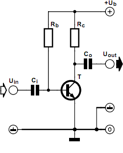

That means, that with a mains voltage of 240 Veff there will be about 340 V DC after rectification and filtering. If in the amplifier circuit the power supply voltage is now 340 V and the collector voltage is 2 V, then the gain is in theory equal to 40 x (340–2). This is more than 13,500 times! However, there are a few drawbacks in practice. This is related to the output characteristic of the transistor. In practice, it turns out that the transistor does actually have an output resistor between collector and emitter.

This output resistance exists as a transistor parameter and is called ‘hoe’. In normal designs this parameter is of no consequence because it has no noticeable effect if the collector resistor is not large. When powering the amplifier from 340 V and setting the collector current to 1 mA, the collector resistor will have a value of 338 k. Whether the ‘hoe’-parameter has any influence depends in the type of transistor. We also note that with such high gains, the base-collector capacitance in particular will start to play a role.

As a consequence the input frequency may not be too high. For a higher bandwidth we will have to use a transistor with small Cbc, such as a BF494 or perhaps even an SHF transistor such as a BFR91A. We will have to adjust the value of the base resistor to the new hfe. The author has carried out measurements with a BC547B at a power supply voltage of 30 V. A value of 2 V was chosen for the collector voltage. Measurements confirm the rule of thumb. The gain was more than 1,000 times and the effects of ‘hoe’ and the base-collector capacitance were not noticeable because of the now much smaller collector resistor.

Author: Gert Baars Copyright: Elektor Electronics
Read More..

Friday, October 3, 2014

Simple Adjustable Voltage Circuit Source With NPN Transistor

It is a simple and less efficient method to control DC voltage is using a voltage divider and transistor emitter follower configuration. The figure below is illustrated use a 1K potentiometer to set the base voltage of a medium power NPN transistor. The collector of the NPN feeds the base of a larger PNP power transistor which supplies most of the current to the load. The output voltage will be about 0.7 volts below the voltage of the wiper of the 1K pot so the output can be adjusted from 0 to the full supply voltage minus 0.7 volts. Using two transistors provides a current gain of around 1000 or more so that only a couple milliamps of current is drawn from the voltage divider to supply a couple amps of current at the output. The figure is;


Note that this circuit is much less efficient than the 555 timer dimmer circuit using a variable duty cycle switching approach. In the figure below, the 25 watt/ 12 volt lamp draws about 2 amps at 12 volts and 1 amp at 3 volts so that the power lost when the lamp is dim is around (12-3 volts * 1 amp) = 9 watts. A fairly large heat sink is required to prevent the PNP power transistor from overheating. The power consumed by the lamp will be only (3 volts * 1 amp) = 3 watts which gives us an efficiency factor of only 25% when the lamp is dimmed. The advantage of the circuit is simplicity, and also that it doesnt generate any RF interference as a switching regulator does. The circuit can be used as a voltage regulator if the input voltage remains constant, but it will not compensate for changes at the input as the LM317 does.

Read More..

Sunday, September 21, 2014

High And Low Voltage Cut Off With Time Delay

High And Low Voltage Cut Off With Time Delay The power line fluctuations and cut-offs cause damages to electrical appliances connected to the line. It is more serious in the case of domestic appliances like fridge and air conditioners. If a fridge is operated on low voltage, excessive current flows through the motor, which heats up, and get damaged.

The under/over voltage protection circuit with time delay presented here is a low cost and reliable circuit for protecting such equipments from damages. Whenever the power line is switched on it gets connected to the appliance only after a delay of a fixed time. If there is hi/low fluctuations beyond sets limits the appliance get disconnected. The system tries to connect the power back after the specific time delay, the delay being counted from the time of disconnection. If the power down time (time for which the voltage is beyond limits) is less than the delay time, the power resumes after the delay: If it is equal or more, then the power resumes directly.

This circuit has been designed, built and evaluated by me to use as a protector for my home refrigerator. This is designed around readily available semi-conductor devices such as standard bipolar medium power NPN transistor (D313/SL100/C1061), an 8-pin type 741 op-amp and NE555 timer IC. Its salient feature is that no relay hunting is employed. This draw back is commonly found in the proctors available in the market.

The complete circuit is consisting of various stages. They are: - Dual rail power supply, Reference voltage source, Voltage comparators for hi/low cut offs, Time delay stage and Relay driver stage. Lets now look at the step-by-step design details.

Dual rail power supply.

This is a conventional type of power supply as shown in Figure 1. The power is applied through the step-down transformer (230/12-0-12V/500mA). The DC proportional to the charging input voltage is obtained from bridge rectifier. Two electrolytics are there to bypass any spikes present. Bridge is capable of handling currents up to 1 Amp.

Output is given by: -

V(out) = 0.71 X V (secondary)

= 0.71 X 24V

= 17.04 V

(This equation is similar for the negative rail as well)

Circuit diagram

Low voltage cut off op-amp

Figure 2 shows the use of very common and easily available op-amp 741 as a comparator. The op-amp is available in TO-5 and DIP type packing.

Circuit diagram

In this ckt the zener diode D1 and it’s associated resistor R1 are connected to the non-inverting terminal (+ve) of 741 to give the suitable reference voltage. The DC voltage from the sensor is given to the inverting (-ve) terminal through pre-set R2.This is used to set the input level.

When the sensor input is less than Zener voltage the output from the Op-amp remains high and when it is greater than Zener voltage the output goes low. When the sensing voltage is equal to Zener voltage the output of the op-amp is approximately zero.

This phenomenon is used as a decision for switching the relay and to give cutoff in a low voltage situation.

High voltage cut off op-amp

Here the op-amp is used as a inverted amplifier. See Figure 3.Zener and resistor network gives reference voltage to the inverting terminal (-ve) of op-amp. Sensing voltage derived through the 10 K pre-set is given to the non- inverting (+ve) terminal and this sets the high level cut.

When the input DC from the sensor is less than Zener voltage the output of the op-amp is low and vice-versa. When the input DC voltage is equal to the zener voltage, the op-amps output is approximately zero.

Circuit diagram

Time delay

I’ve selected the 555 timer due to following reasons.

1. Timing from microseconds through hours.

2. Ability to operate from wide range of supply voltages.

3. High temperature stability.

4. Easily Available.

5. Its triggering circuit is quite sensitive.

This is basically a monostable. The external timing capacitor C2 is held initially discharged by the timer. The circuit triggers upon receiving a pulse to its pin 2 when the level reaches 1/3 Vcc. Once triggered., the circuit will remain in that state until the set time is elapsed or power to the circuit cuts off. The delayed period in seconds is 1.1 C2.R1 where R1 is in megohms and C2 is in microfarads. In practice, R1 should not exceed 20 M. If you use an electrolytic capacitor for C2, select a unit for low leakage. The time delay may have to be adjusted by varying R1 to compensate for the wide tolerance of electrolytics.


Circuit diagram

Relay Driver

The output from the voltage level detectors cannot directly drive the relay and hence the relay driver is used.

Circuit diagram

In this a relay (12V <500 ohms) is connected to the collector of npn transistor. the out put voltage from the comparator is applied to the base of npn transistor through a resistance r1. when the output from the comparator is low the transistor is in off state and the relay is in de-energized state. similarly when the output from the comparator goes high the transistor switches on and the flow of current from the collector to emitter of transistor energizes the relay.

Generally in a relay driver circuit, parallel to the relay coil, a diode or a capacitor is used. This is to eliminate the back e.m.f generated by the relay coil when currents are suddenly broken. Capacitor C1 is connected in parallel to the coil, which filters out the back emf but it, slows down the working of relay.

A better method is to connect two diodes (as shown in the figure 5) that stop the relay – transistor junction swinging more than 600mV above the positive rail or below the zero-volt rail. During normal operation the diodes are reverse biased and have no effect on the performance of circuit. But when back emf is induced, the diodes conduct heavily and absorb all transient voltages. However, I have employed the both methods.

The Complete Circuit

Circuit diagram

Under normal operating conditions i.e. when the input voltage is between maximum and minimum limit the output from the both the comparators are low. The transistor Q1 is OFF and the relay is in de-energized (pole connected to N/C pin) state and the output is obtained.

When the input voltage is below or above the limits set by the pre-sets R8 or R9, the output of the Op-Amps goes either low or high and diodes D1 or D2 would be forward biased depending on the situation. Transistor Q1 switches ON and the flow of current from collector to emitter energizes the relay and the output is cutoff.

A small amount of hystersis has been added via feed back resistors R10 & R11 so that the relay turns on when the level falls to a particular value but does not turn again until it raises a substantial amount above this value. Other wise the relay contacts will frequently turn on/off and produce chattering.

Construction Hints

1) I used a piece of varoboard, which has copper strips on one side to mount the components, and housed the entire circuit and the transformer in a discarded ATX PC power supply box.

2) An autotransformer has been used to set the limits. Set the output of the autotransformer to 250V AC and connect it to the primary of transformer T1 (see Figure 1). Then adjust the pre-set R9 such that relay just energizes. This is the high limit. Next set the output of the autotransformer to 200V AC and adjust the pre-set R8 such that the relay energizes. Please note that these are my preferred limits but you may select any range from say 170 to 270V AC.

3) A neon with a suitable resistor could be connected between the AC supply lines as an ON indicator. Alternatively, LED with a current limiting resistor could be connected between the relay coil so when the relay is energized LED will indicate the situation. 

Read More..

Thursday, September 18, 2014

140W audio amplifier with IC STK070

By using the above amplifier circuit you can hear the sound quality is quite good by a high output power. Maximum voltage circuit pa approximately 55Volt DC. 70-140W output power with impedance 8Ohm.
power
Read More..

Monday, September 8, 2014

25W Bridge Audio Amplifier with TDA2005

This is the 25W bridge audio amplifier built using single power IC TDA2005. Actually, the TDA2005 is a stereo power amplifier chip. It has two input channels and two output channel and delivers about 10W power output for each channel, since it connected in bridge mode then it will delivering up to 25W audio output. Take a note that the speaker terminals should not conected to the ground and mount the IC on the heatsink to prevent overheating.

 25W Bridge Audio Amplifier with TDA2005 Circuit Diagram


25W

Parts List:
R1 = 120K?
R2,5,6 = 1K?
R3,4 = 12?
R7,8= 1?
C1,5,7 = 220uF/25V
C2,10,11 = 100nF
C3,4 = 2.2uF/25V
C6,8 = 100uF/25V
C9 = 10uF/25V
IC1 = LM2005M / TDA2005
Read More..

Friday, September 5, 2014

Easy Using LM317 with Over voltage Protection

The schema diagram shows the over voltage protection as a feature of LM317 linear voltage regulator.Over voltages come from several source or factors which are usually in the form of transients. Transients are represented in spikes which are short and fast disturbance or change in the voltage and current component.

It only occurs in diagram containing conductance and capacitance. The causes are typically from power outages, short diagram, tripped schema breakers, lightning spikes, inductive spikes and other malfunctions from power company.


 As an example using a 12V battery source, the LM317 voltage regulator can be used to obtain 6 Volts. To protect any device from over voltage, there are ways such as adding relays or a zener diode. A relay switch functions by opening or closing under the command of another schema. But finding a relay that would limit the output from 6 V to 12 V is not easy.

Fortunately, zener diodes are more abundant. A 6.2V zener diode rating can be used to surpass any excessive voltage set by the voltage regulator, to prevent more damage to the schema. The components will be as follows:

ZD1 – 6.2 Volts
R1 – 1K ohms
R2 – 1K ohms
T1 – NPN Transistor (low power)
T2 – NPN Transistor (acts as a switch)

Every schema design needs to be tested carefully as to avoid further damage to the equipment that will be connected. The trial can be done by using a multimeter, and gradually increasing the schema voltage. Once the schema turns off the supplied voltage, take note of the reading which will signify the threshold voltage of the zener diode.
Read More..