Monday, January 26, 2015

123 Game All MCU free

This electronic game pits a human player against the ‘machine’. The opponents use a common ‘game token’ and take turns moving along a path by one, two or three steps, and the winner is the first one to reach the goal exactly. Incredibly enough, this simple version of the ‘123’ game can be built without a microcontroller, and it’s almost impossible to beat. The electronics for this is built using only diode logic (Figure 1). The ‘ input inter face’ consists essentially of 30 miniature sockets to which a probe tip can be connected to mark the position of the ‘game token’.

To make the game more compact, the sockets are arranged in a grid so the route along the sockets follows a serpentine path (Figure 2). The starting position is at the bottom right, and the goal is in the middle of the playing area. The electronics becomes the ‘active player’ when the button is pressed.

The number of steps it wants to move is shown by three LEDs (one, two or three LEDs light up) at the top of the playing area. Naturally, the human player must move the ‘game token’ for the machine opponent. The winner is the first one to reach the goal exactly. How can such simple circuitry represent such a formidable opponent? As already mentioned, the path from the start to the goal is formed by 30 sockets. Each socket has an associated ideal next move. 

There are three possibilities, of course: 1, 2 or 3. As you can see from the schematic diagram, switch S1 closes the circuit (which means the player asks the ‘computer’ how many steps it wishes to move) if the probe is touching one of the sockets. All 30 sockets are classified into three types, represented in the schematic diagram by one socket for each type. All sockets belonging to a particular type are simply connected together electrically, which is not shown on the schematic diagram for the sake of clarity.

Circuit Diagram:


This is how the LED display works:

The player touches the right-hand contact with R4 (only LED D3 lights up), the left-hand contact with R3 (LEDs D1 and D2 light up), or the middle contact with diodes D4 and D5 (all three LEDs light up). The two diodes prevent all three LEDs from lighting up if the player touches the left-hand or right-hand contact. The key to all this lies in the assignment of the 30 sockets to the three types of logic, which means the three types of ideal next move. 

Working backward from the goal, no further move is possible when the goal is reached. For this reason, the last socket is not connected to anything. At the socket just before the goal, the ‘computer’ naturally wants to be exactly one step in front. Consequently, this socket is connected to R4. At the second socket before the goal, the electronics wants to move by two steps. This socket is thus connected to R3.

Obviously, three moves before the finish, a three-step is best as it leads to instant victory. Consequently this socket is connected to D4/D5. The correct response of the ‘computer’ is shown in Figure 2 by the number next to each position. As the two opponents take turns playing, the electronics always tries to arrive at a strategically favourable position (marked by the arrows). If the electronics manages to reach one of these positions, it’s impossible for the human player to win. This means that the human player can only win by starting first and always making the right move.
Read More..

Sounds From The Old West Using IC1 HT82207

This circuit shows how far integration can be taken: IC1, a Type HT82207 from Holtek does virtually everything. Only a (small) loudspeaker and the necessary selectors need to be added. The standard 18-pin Type HT82207 is an integrated sound generator, producing sounds typical of the Old West. The various sounds are selected by S1–S6 as listed below. In the quiescent state, the circuit draws a current not exceeding 1 µA.
  • S1 – bugle
  • S2 – neighing
  • S3 – sound of hooves
  • S4 – pistol shot
  • S5 – crack of a rifle
  • S6 – cannon fire
Sounds From The Old West Circuit Diagram:

Read More..

Friday, December 12, 2014

Battery Charger for NiCad Batt

charger

This battery charger circuit is designed for recharging NiCad batteries based on an AC-powered current source method.It can crank out as much as 1 amp and can be modified to go even higher by choosing different devices for Q1. Since this circuit uses AC line voltages and currents, please exercise extreme caution during assembly, turn-on, and test. 
Read More..

Wireless Transmitter for IR Headphone

This circuit shows a Wireless Transmitter for IR Headphone.
Read More..

Dual Voltage Inverter

This voltage inverter schematic can produce a dual (positive and negative) voltage from a single supply input.It is therefore extremely useful for powering opamp and other circuits that require a dual voltage from a single battery. The circuit will operate at an input voltage from around 5V to 20V and produce a output from +-2.5V to +-10V. 
Read More..

Thursday, December 11, 2014

Car Laptop Power Supply Adaptor
laptop-adaptor-schematic
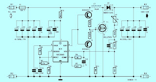
The laptop adaptor described here plugs into a car cigarette lighter socket and produces a 19V nominal output voltage adjustable by + - 0.5V. The input voltage range is from 9.2V to 15V and the output voltage shows good regulation even with large fluctuations of the input voltage. 
Read More..

Thursday, November 20, 2014

1 Lamp with 2 switches

Series 1 light 2 switch configuration is intended to control lights from two locations arefar apart. Application of series 1 light with 2 switches are often implemented in thehallway or tunnel. In the application in a hallway or tunnel, with a series like this we can turn on or turn off the light from each tunnel or hallway door. The number of lights can bereproduced by paralleling. The circuit is very simple because only built of 1 and 2pieces of fruit lamp selector switch. If you want to use a lamp with a power greater then the switch can be replaced with 1 piece contactor (relay) for each switch. Then switchused to turn on and turn off the relay replacement S1 and S2.

The working principle with 2 series 1 light switch is the light will light when the S1 and S2 different position, and the lights will be on at the time of the switch position S1 and S2 together. In the installation of switches S1 and S2 each put at the end of the hallway or tunnel.
Read More..

Mini Amplifier with 3 Transistor

Mini 3 transistor amplifier is a simple amplifier with 50mW power drawn by 3 transitor.
The series of three mini-amplifier transistors can be used for loud speaker 8 ohm load. Source voltage required to activate the mini-amplifier can be drawn from the batteries 9V.Rangkaian 3 transistor amplifier is often used in simple portabe audio devices such as radios or small tape recorder. Mini-transistor amplifier circuit 3 is quite simple as shown in the figure below.


Mini


Mini-transistor amplifier circuit 3 includes type of amplifier OTL (Output Transformer Less). Mini-transistor amplifier circuit 3 is used for output coupling capacitors. Amplifier circuit is simple and suitable when used for audio amplifier experiment.
Read More..

Improving Performance Bass Amplifier

Stereo power amplifier is less in the bass tones, but if a speaker that sounds just feels solid bass sound, there are several possibilities, the first one speaker cable upside down, try alternating bass and tone tests.
If still, you need to use 2 power supply or attempting to use this circuit. Note this circuit works for a power amp that is less power transformer with 2 speakers (stereo). One of the speaker cable (output) should be reversed, this is okay, just a game to lighten the work phase transformer from the blow bass.
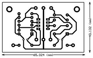
We recommend that before you try this circuit, turn one speaker cable and a second test speakers with bass tones, the bass should be mutually reduce (bass-bass = 0). Next remove the driver from boknya and turn the speakers (the speaker drivers facing into the wall), the bass should grow (bass + bass = 2bass). One record store in the town of Indramayu is taking this simple way, certainly looks magnet speakers, great.

The heart of this circuit using IC with 2 op-amps, can type JRC4558, LF353, TL072, TL082, and similar. Vcc = + /-70Vdc. If Vcc = + /-42Vdc, replace the value of R9 and R10 to 2K2.
Op-amp 1 functions as a buffer, while the op-amp to-2 function as inverting the phase 180 , both have a reinforcement of 1 times.

Improving

Improving

List of components:
R1, 2,5,6 .......... 100K
R3, 4 ................ 2K2
R7 ................... 100
R9, 10 .............. 2K2-3K3
C1, 2 ............... 100uf/25V
D1, 2 ............... 15V Zener
IC1 ................. TL072
Read More..

Wednesday, November 19, 2014

TDA 7012T FM Radio Receiver

FM Radio Receiver IC TDA 7012T is very simple, but it has an FM radio receiver sensitivity and good selectivity. Single Chip FM Receifer cool name of IC TDA7012T 7012T TDA is to build an FM receiver requires a few additional components. Feature contained in FM receiver IC TDA 7012T is quite tempting to an FM receiver. Among features an FM receiver TDA 7012T is a low-voltage applications micro affability arrangement (MTS), Frequency Loked Loop (FLL) to 76 KHz range and selectivity of FM receiver with RC Filter. In an article by FM Radio Receiver IC TDA 7012T can be seen in the FM receiver circuit which can be made​​.
 
Image Series FM Radio Receiver with IC TDA 7012T


From the picture above components to make the FM Radio Receiver IC TDA 7012T as follows:

R1 = 8kΩ2
R2 = 10kΩ
R3 = 390Ω
C1, C3 = 10nF
C2, C6, C9, C16 = 100nF
C4 = 33pF
C5 = 25pF trimmer
C7, C10 = 1nF5
C8 = 820pF C11 = 1NF
C12 = 68pF
C13 = 220pF
C14 = 47μF 10V
C15 = 3nF3
L1 = 36nH
L2 = 1μH,
IC1 = TDA7021T

Hopefully useful and become an idea in the manufacture of Mini FM Receiver with IC TDA 7012T
Read More..

Programming Learning MCS51

Learning Programming MCS51 becomes mandatory we learn if we want to use the MCS51. In the first part of this Learning Programming MCS51 we will learn together about the basic programming language MCS51 microcontroller. Where to program MCS51 outline there are 2 core parts of pemrogramanya language is "Words Work" and "Object". In the article Programming MCS51 this first part we will study first the "verb" is a command group Peng-copies of data, the command group arithmetic and logic command group.

Programming
Reference to DATA IN PROGRAMMING MCS51
Data can be in many different places, thus known a few ways to describe the data (in English often referred to as Addressing Mode), among others, as follows:

The mention of constant data (immediate addressing mode): MOV A, # $ 20. Constant data is data that was in the instructions. Examples of this instruction has the data meaning a constant $ 20 (as a constant data marked with #) on-copy it into the accumulator A. What needs to be properly addressed in this order is the number $ 20 is part of the instruction.
Reference to data directly (direct addressing mode), this method is used to refer to data residing in memory by calling the memory number where the data are: MOV A, $ 30. Examples of these instructions have the meaning of data in the memory number $ 30 in-copy it to the accumulators.
At first glance these same instructions to the instruction constant data above, the difference above instructions using the # which marks the $ 20 is a data constant, whereas in this instruction because there was no sign # then $ 30 is a number from memory.

The mention of indirect data (indirect addressing mode), this method is used to refer to data residing in memory, if memory data storage is changing its location so that the memory number is not called directly but in-titip her into another register : MOV A, @ R0.
In this instruction versatile R0 register is used to record the number of memory, so that this instruction has a memory meaning that the number recorded in the contents of R0-copy it into the accumulator A.

Sign @ is used to mark the memory number stored in R0.

Compare this with the instruction memory number directly mention above, in this instruction first memory numbers are stored in R0 and R0 appoint a role which memory is used, so that if the value of R0 change the designated memory will also be changed as well.

In this instruction registers R0 functioning multipurpose container for the address register (indirect address register), other than all-purpose registers R0 R1 can also be used as a container for the address register.

Reference to data in the register (register addressing mode): MOV A, R5. This instruction has the meaning of data in all-purpose register R5 is copy it into the accumulator A. This instruction makes all-purpose registers R0 to R7 as a place to store data that is very practical that it works very fast.
The data referred to in the discussion above all in the data memory (including all-purpose registers are also located in data memory). In writing the program, often required standard table that is stored along with the program. Tables of this kind is really a data residing in program memory!
For this purpose, MCS51 have any mention of data in memory means programs conducted by indirect (indirect addressing code mode): MOVC A, @ A + DPTR.

Notice in this MOV instruction is replaced with MOVC, the additional letter C is meant to distinguish that this instruction is used in the program memory. (MOV without the letter C means that the instruction used in the data memory).

Sign @ is used to mark A + DPTR is used to indicate the number of contents in-memory copy it to the accumulator A, in this case the value stored in the DPTR (Data Pointer Register - 2 bytes) plus the value stored in accumulators A (1 byte) is used to refer to the program memory numbers.

Verb in AT89Cx051
Overall AT89Cx051 have as many as 255 kinds of instruction, which was formed by combining the verb and objects. "The verb is the group discussed the following:

PENG GROUP-COPY-DATA AN MCS51
Basic code for this group are MOV, abbreviation of MOVE, which means to move, though more correct to say this command have meaning copying the data. This can be explained the following: after the instruction MOV A, R7 done, accumulators A and all-purpose register R7 contains the same data, originally stored in R7.

MOV command is distinguished according to the type of memory AT89Cx051. This command is on the memory data is written into MOV, for example:


MOV A, $ 20

MOV A, @ R1

MOV A, P1

MOV P3, A

To use the program memory, this command is written into MOVC, there are only 2 types of wear MOVC instructions, namely:


MOVC A, @ A + DPTR; DPTR as register indirect

MOVC A, @ A + PC, PC as the register indirect


In addition, there is also known MOVX command, the command that is used for external data memory (X singkatakan from External). This command is only available to the MCS51 family members who have an external data memory, for example AT89C51 and so forth, and certainly not known by the group that tidam AT89Cx051 have external data memory. There are only 6 kinds of wear MOVX instruction, these instructions are:


MOVX A, @ DPTR

MOVX A, @ R0

MOVX A, @ R1

MOVX @ DPTR, A

MOVX @ R0, A

MOVX @ R1, A


GROUP ARIMATIK (ADD, ADDC, SubB, DA, MUL and DIV)
ADD and ADDC command

The contents of accumulators A plus the number 1 byte, the sum will be collected back in the accumulator. In this operation Carry bit (C flag in the PSW - Program Status Word) serves as a reservoir overflow of the sum. If the sum of the abundance (a value greater than 255) will carry bit value 1 , if not Carry bit value 0. ADDC same with ADD, only in bits Carry ADDC value in the previous process involved summed together.

Numbers 1 byte is added to the accumulator, can be derived from a constant, from the all-purpose register, memory data from memory number is called directly or indirectly, as shown in the following example:

ADD A, R0; register versatile

ADD A, # $ 23; a constant

ADD A, @ R0; no memory indirect

ADD A, P1; no direct memory (port 1)


ORDERS IN PROGRAMMING SubB MCS51
The contents of Accumulator A less the number 1 byte follows with Carry bit value, the reduction will be accommodated again in the accumulators. Carry bits in this operation also serves as a reservoir overflow of the reduction. If the reduction is abundant (score less than 0) bits Carry would be worth 1 , if not Carry bit value 0.

SubB A, R0; A = A - R0 - C

SubB A, # $ 23; A = A - $ 23

SubB A, @ R1

SubB A, P0


DA command

DA command (Decimal Adjust) is used after the command ADD, ADDC, or SubB, used to convert 8-bit binary value stored in the accumulator into 2 pieces decimal number, each consisting of 4-bit binary value.

MUL AB ORDERS IN PROGRAMMING MCS51
8-bit binary number in accumulator A is multiplied by an 8-bit binary number in register B. The result of multiplication of binary 16-bit, 8 bit binary number that greater weight be accommodated in the register B, while the other 8 bits are accommodated in the smaller weight accumulator A.

OV bit in the PSW (Program Status Word) is used to mark the result of multiplying the existing value in register B. OV bit will be worth 0 if register B is worth $ 00, if not worth OV bit 1.

MOV A, # 10

MOV B, # 20

MUL AB

DIV AB ORDERS IN PROGRAMMING MCS51
8-bit binary number in accumulator A is divided by an 8-bit binary number in register B. The result of the division of 8-bit binary numbers stored in the accumulator, while the rest of the division of 8-bit binary number stored in register B.

OV bit in the PSW (Program Status Word) is used to mark the value before the division that exists in the register B. OV bit will be worth 1 if register B originally worth $ 00.

GROUP LOGIC (ANL, ORL and XRL) IN PROGRAMMING MCS51
This command group used to perform logic operations MCS51 microcontroller, logic operations can be done is the AND operation (operation code ANL), OR operation (operation code ORL) and the Exclusive-OR operation (XRL operation code).

The data used in this operation can be data that is in the accumulator or data that are in-memory data, this is a little different with arithmetic operations that must be actively melihatkan accumulators.

Operating results are accommodated in the first data source.

AND logic operation is widely used to me 0 a few specific bits of an 8-bit binary number, the way to forming an 8-bit binary numbers as a data-ANL constant in a number of origin. Bit-0 want in a represented by 0 in constant data, while other bits given the value 1, eg
Instructions ANL P1, #% 01111110 will result in bit 0 and bit 7 of Port 1 (P1) value 0 while the other bits remain unchanged in value.

OR logic operation is widely used to me 1 a few specific bits of an 8-bit binary number, the way to forming an 8-bit binary numbers as constant data in a number-ORL origin. Bit-1 want in a represented by 1 in constant data, while other bits given the value 0, eg
Instructions ORL A, #% 01111110 will result in bit 1 to bit 6 of the accumulator value 1 while other bits remain unchanged in value.

Exclusive-OR logic operation is widely used to reverse the value (complement) some particular bits of an 8-bit binary number, the way to forming an 8-bit binary numbers as constant data in a number-XRL origin. Bit you want behind-the value represented by 1 in constant data, while other bits are the value 0, eg
Instructions XRL A, #% 01111110 will result in bit 1 to bit 6 of the accumulator turned value, while other bits remain unchanged in value.
Read More..

Adjustable Switching Regulator Circuit with LM2576

The Adjustable Switching Regulator Circuit with LM2576 are monolithic integrated circuits that provide all the active functions for a step-down (buck) switching regulator, capable of driving 3A load with excellent line and load regulation. These devices are available in fixed output voltages of 3.3V, 5V, 12V, 15V, and an adjustable output version.
LM2576 IC Package
Requiring a minimum number of external components, these regulators are simple to use and include internal frequency compensation and a fixed-frequency oscillator. The Adjustable Switching Regulator Circuit with LM2576 offers a high-efficiency replacement for popular three-terminal linear regulators. It substantially reduces the size of the heat sink, and in some cases no heat sink is required.


IC Switching Regulator Circuit with LM2576

A standard Adjustable Switching Regulator Circuit with LM2576 of inductors optimized for use with the LM2576 are available from several different manufacturers. This feature greatly simplifies the design of switch-mode power supplies.

Other features include a guaranteed ±4% tolerance on output voltage within specified input voltages and output load conditions, and ±10% on the oscillator frequency. External shutdown is included, featuring 50 μA (typical) standby current. The output switch includes cycle-by-cycle current limiting, as well as thermal shutdown for full protection under fault conditions.

Features Adjustable Switching Regulator Circuit with LM2576 :
- 3.3V, 5V, 12V, 15V, and adjustable output versions
- Adjustable version output voltage range,1.23V to 37V
- Guaranteed 3A output current
- Wide input voltage range, 40V up to 60V for HV version
- Requires only 4 external components
- 52 kHz fixed frequency internal oscillator
- TTL shutdown capability, low power standby mode
- High efficiency
- Uses readily available standard inductors
- Thermal shutdown and current limit protection
- P+ Product Enhancement tested
Read More..

Tuesday, November 18, 2014

Simple fm transmitter for the experiment
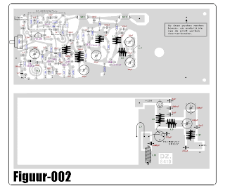
Simple fm transmitter for the experiment. This designation may be appropriate to call this series, because rangkaianya very simple and suitable for learning / beginners. and preferably when assembling, which assembled its first part oscilator. then we try it first. if able to function normally, we can proceed to the next level up to the booster.


Read More..

Solid State Relay Circuit

Solid state relay is a series of hibryd that serves as a mechanical relay. Solid state relays is built with insulating an MOC to separate the input and the switch. Solid state relay with us to avoid the occurrence of sparks as it does on conventional relays can also avoid the occurrence of the connection is not perfect because the porous contactor as in conventional relays. Solid state relay circuit is quite simple and we can make in a PCB hole. For more details can be seen in the picture following a series of solid state relays.


Solid state relay has many advantages including no mechanical friction on the contactor, the connection process only occur when there are crosses zero, there is no spark at the contactor, not noisy, small consumtion flow control, better endurance.
Read More..

Emergency Lights Circuit

The series of emergency lights on this one is a series of emergency lighting is quite simple and not difficult to make. 

Emergency

Frankly this circuit is not my own design, but at least this series can add to your collection of electronic circuits. The circuit is actually almost the same as the battery charger circuit, its just that in this emergency coupled switching circuit as a circuit breaker when the circuit load is connected to the supply voltage of 220 volts or in other words on the charging position. Meanwhile, when the voltage of 220 volts is lost (PLN lights off), then automatically switches the load switching circuit and turn on emergency lights, where the supply that is used is derived from batteries that have been installed in stand-by position.

In a series of emergencies over the use of LED as a lighting load emergency. And indeed these days we find a lot of emergency lights that are sold in the market that use LEDs, but the LED is used instead led carelessly but has led a gleam of light. The advantages of the use of this led the led is very efficient because once will consume battery power so that with a limited supply to run the series in a long time.

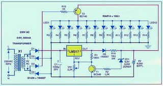
Circuit components used for emergency lighting is not too much, and indeed the components used are the components that are commonly used as components for circuit switching power supply and battery charging. IC LM 317 ic regulator is useful as a producer of supply voltage to supply the batteries. Transistor T2 (BD 140) is useful as switching, ie, decide the flow toward the load at 220 volts PLN lamp life so that lighting will be extinguished. But when the lights PLN did not provide the supply voltage of the transistor T2 will connect the connection from the battery to the load light.

Components used:
Resistors: R1 (180 uhm), R2 (1.2 K), sd R3 R14 (100 ohms), R15 (1 K) and R16 (16 ohm, 5 watt)
Capacitors: C1 (1000 UF)
Diodes: D1 until D5 (IN 4007)
Transistors: T1 (BC 548) and T2 (BD 140)
Zener Diodes 6.8 Volt
IC: LM 317
Battery charger
Transformer
If you are not happy using this type of charger with IC LM317 series like the example above then you can use another type of charger circuit that you think is more appropriate and can work optimally. Then you simply add the switching function by using one or more transistors.
Read More..

POWER SUPPLAY 13 8 Volt Schematic

POWER
POWER
POWER
POWER

Part list for 12 Amp BDX33-based power supply:

  • 2 x 15 volt 6+ amps

  • 2 times two MR750 (MR7510) diodes (MR750 = 6 Ampere diode) or 2 times 3 1N5401 (1N5408) diodes.

  • F1 = 1 Amp

  • F2 = 15 amp

  • R1 2k2 1 Watt

  • R2 10k

  • R3 1k 0.5 watt

  • R4,R5,R6,R7 0.1 ohm 10 watt

  • R8 4.7

  • R9 6k8

  • C1 two times 4700uF/35v

  • C2 330uF/35v

  • C0,C3,C4,C6,C10 100nF

  • C7 330uF/25v

  • C8 47nF

  • C9 47uF/25v

  • D1 1N5401

  • D2 LED

  • D3, D4, D5 1N4001

  • IC1 78L15

  • relay 12 volt 2x5 amp switching

  • 3 darlington transistors: T0,T1,T2 = BDX-33 NPN TO-220 transistor

  • Zd 8 or 9 volt, 5 watt

  • P1 2k trimmer

If using a bridge rectifier (like in schematic 2) you do not need 2 x 15 volts 6 amps, but 1 x 15 volt 10+ Amps

Part list for 20 Amp BDX33-based power supply:

  • 2 x 15 volt 12+ amps

  • 2 times 3 MR750 (MR7510) diodes (MR750 = 6 Ampere diode) or 2 times 5 1N5401 (1N5408) diodes.

  • F1 = 2 Amp

  • F2 = 25 amp

  • R1 2k2 1 Watt

  • R2 10k

  • R3 1k 0.5 watt

  • R4,R5,R6,R7 0.1 ohm 10 watt

  • R8 4.7

  • R9 6k8

  • C1 22000uF/35v

  • C2 330uF/35v

  • C0,C3,C4,C6,C10 100nF

  • C7 330uF/25v

  • C8 47nF

  • C9 47uF/25v

  • D1 1N5401

  • D2 LED

  • D3, D4, D5 1N4001

  • IC1 7815

  • relay 12 volt 10 amp switching

  • Four darlington transistors: T0,T1,T2,T3 = BDX-33 NPN TO-220 transistor

  • Zd 8 or 9 volt, 5 watt

  • P1 2k trimmer

If using a bridge rectifier (like in schematic 2) you do not need 2 x 15 volts 12 amps, but 1 x 15 volt 20 Amps

Read More..

Monday, November 17, 2014

Boster 15 watt rd 15 no tune

15 rd booster requires only 0.5 watts of input capable of out 15 watts, the voltage of 13.8 volts it needs. in this series are made to work freq 87-108 mhz fm broadcast. but did not rule to be modified in other freq. schematic and pcb layout to please download here


Read More..

Radio Control for toy car

play toy cars controlled by radio signals is an interesting game. The much-loved toy cars children, plus a simple circuit would be ideal for toy cars. This series of families use traditional digital CMOS IC which requires a very small electric current, so it does not impose on the performance of the original toy cars.
In this system, radio signals emitted not continuously but only generated when the controller sends a command left / right or forward / backward, and even then only a radio frequency of an intermittent, so it is sending pulses of radio wave frequency.

Number of pulses sent represents a command is sent, the command GO is represented by 8 pulses, represented by 16 pulses LEFT, RIGHT DOWN 32 pulses and 64 pulses. Command sent to a combination of two orders once gus, which is a combination of command forward / backward and right / left, for example, could be sent forward command and left once gus, in this case the number of pulses sent is 24, which is the sum of the forward command command as much as 8 pulses and left as many as 16 pulses.
Once a command is sent, the system stops sending commands in a certain time lag, the lag time it takes the receiver circuit will have sufficient time to execute properly. Frequency pulses were visible on the right side of Figure 1.

How it works The transmitter
Radio signals generated by the oscillator circuit formed by transistors Q1 9016, the working frequency of the oscillator is determined by the crystal Y1 is worth 27.145 MHz. A very critical part of this oscillator circuit is T1, L1 and L2, which specifically dealt with separately at the end of this article.
Work of the oscillator is controlled by a NOR gate U2D 14001, while the output gate (pin 3) is worth 1 , the oscillator will work and transmit radio frequency 27.145 MHz, and at the output U2D value 0 the oscillator will stop working.
U2D NOR gate receives the clock signal from the NOR gates U2B. NOR gate CMOS type with the help of resistors R4 and R5 and capacitor C8 to form a low frequency oscillator circuit to control the clock shaper of existing digital circuits. Working from the clock generator is controlled via the input leg 6, the circuit will generate the input clock that is berlevel 0 .
NOR gate U2A and U2C form a latch circuit (RS Flip Flop), due to the influence of resistor R2 and capacitor C11 which is fed to pin 9 on U2C, when the circuit gets power supply output U2C must be 1 and U2A output (pin 3) to 0 . This situation resulted EUIS clock generator generating a clock U2B work and release the reset state of the enumerator 14 024 IC (U1), so that the U1 start chopping and 27.145 MHz oscillator circuit to send pulses of the clock generator frequency during work.
At the start chopping, all the output IC 14 024 enumerators in kedaan 0 , after chopping the 8 pulse output Q4 (pin 6) will be 1, after chopping 16 Q5 pulse output (pin 5) to 1 , after chopping 32 Q6 output pulse (pin 4) to 1 , after 64 counts pulses output Q7 (pin 3) to 1.
Outputs are used to control the voltage above 9 feet U2C through diode D1 and D2, as long as it remains one of the output value 0 then the plant U2B clock still works, it will continue until dankatode D2 D1 cathode to 1 so that the foot 9 U2C a 1 as well. This situation will lead to 3 feet U2A output to 1 , which stops the clock generator and reset U2B enumerator 14 024 danberhenti is sending pulses of frequency 27 145 MHz.
To generate the lag time for the receiver circuits have enough time to perform the command, used a series of 9014 Q2, the resistor R7 and capacitor C10. The magnitude of the delay time is determined by the value of R7 and C10. The switch to send the command forward / backward and to send the command left / right are two separate switches. Each switch has three positions, the center position means that the scalar does not send commands.
How It Works Recipients
Figure 2 is a recipient of a series of paired images dimobil toy, serves to receive signals from the transmitter to control the motor cars, so cars can move forward / backward and left / right. Transistor Q1 with the help of resistors; capacitors and T1 form as a series of 27.145 MHz radio signal receiver. T1 in series with a T1 is exactly the same used in the transmitter circuit, how to make it are discussed below.
Transistor Q2 perlangkapannya formed following a series of pulses to change the radio frequency received from the transmitter into the box pulses that can be accepted as a digital signal by the CMOS IC. Digital signal will be received as the clock had to be chopped by enumerator 14 024 IC (U2). Output of 14 024 would correspond to the number of pulses sent by the transmitter, forward command and left (which is used as an example in the discussion of the transmitter) is the pulse number of 24, the enumeration of these pulses resulted in 14 024 to be output Q4 = 1 , Q5 = 1, Q6 = 0 and Q7 = 0.
The received digital signal other than U2 used as counter clock IC 14 024 discussed above, is also used to move the 3 pieces of the time delay circuit to generate pulses which controls the sequence of work.
The first control pulse will appear after submission frequency pulse stopped because the lag time between sending the code, this pulse count function to record the results of 14 024 to 14 042 U3 (D Flip Flop), so that the final condition of 14 024 will be retained to control the motor. After the results were recorded for 14 024 14 042, 14 042 counter is reset by the second pulse, so that after the lag time counter counts up starting from 14 042 to 0 again.
Circuit formed by transistors Q3, Q4, Q7, Q8, Q9 and Q10 H Bridge is named as a series, this series is very powerful to drive the DC motor. With this circuit the DC motor can be rotated to the right-to-left or stop motion. The main requirement is the use of this circuit Q7 and the base voltage of Q10 base voltage must be opposed, for example, the base Q7 = 1 and the base of Q10 = 0 motor rotates to the left, the base of Q7 = 0 and the base of Q10 = 1 motor will turning to the right, the base Q7 = 0 and Q10 base = 0 motor stop motion, but should not be happening base Q7 = 1 and the base Q10 = 1.
Similarly, Q5, Q6, Q11, Q12, Q13 and Q14 form an H Bridge. H Bridge to the left in Figure 2 is used to control a motor that regulates the movement of cars left / right, while the H Bridge to the right is used to control a motor that regulates the movement forward / backward cars.
The relationship between outpur enumerator 14 042 and input D Flip Flop 14 024 is arranged such that the signal is fed to each of the H Bridge can not be all 1 simultaneously.


Manufacture of transformer TX and RX
Transformer T1 in the series transmitter and receiver, is the same stuff, and have made ​​themselves. Transformer was built using a plastic transformer Koker (spare part radio) that has a step that appears 5 lines that can be filled with coils of wire, as shown in the photograph. Wearing this Koker facilitate wire transformer windings. Otherwise it could be similar Koker, just the usual wear. Koker is a small transformer and feritnya also small (3 mm) as that used to be used for the assembly of CB 27 MHz radio.
Can wear a wire to wire the transformer in the unloading of Koker, carefully open coil of wire that already exist in the Koker because the wire is quite smooth and quite easy to break.
Step 1: rolls of wire which is numbered 5 feet to 4 feet in the direction of h (CW) for 3 rolls right on level 1 (pathway level above the bottom line)
Step 2: Roll the wire from 1 foot to 2 feet in a clockwise direction as much as 4 rolls right on level 2.
Step 3: Continue the roll (from step 2) in a clockwise direction as much as three quarter roll to 3 feet on three levels. (Can be determined exactly a quarter of the roll, because it has a track kokernya split into 4).
Manufacture of coil L1
Roll of copper wire diameter from 0.3 to 0.5 mm by 10 quarter rolls on Koker diameter of about 4 mm (which will be released) is also in a clockwise direction.
Manufacture of coil L2
Roll of copper wire 0.1 mm diameter by 50 rolls in plastic Koker without ferrite diameter of about 3.5 - 4 mm (look for the plastic material from scrap) is also in a clockwise direction. Long section on liputi rolls along the 5 mm.
Read More..

Complete Home theater set up speakers

Home theaters are getting to be extremely popular among American homes. This modern technology is slowly giving movie theaters a run for their money. Basic knowledge of home theater system and its basic components may be best for people who want to bring home relaxation and entertainment. 

The most important consideration in the design and complete set up of your home theater is the size of the room. The home theater speakers and the other components of your home theater may need to consider the size of the room. Too small rooms for your home theater may not require so many speakers. Only three speakers may be good if the room is quite small. 

Do not overload your small room; you may not be able to get the entertainment and relation you want if you feel overloaded with so many home theater speakers. Because you only need three home theater speakers in your small room, you may need to acquire the high-end brand of home theater speakers to compliment the size of the room and the other equipments for your home theater.

Complete home theater speaker setup
If you have a bigger room however, the basic three home theater speakers may not be enough. You may need to put up to six speakers around the room, you may also consider complimenting your home theater speakers with subwoofer to complete the surround sound like in movie theaters. In addition to the speakers, you may also need to purchase a high-end television set which should not be smaller than 27 inches. It may not be reasonable if you buy a smaller television set because it may drown in the fineness of your home theater speakers.


Additionally, the DVD player needs to be of high quality, having progressive scan your DVD Player may help provide sharp images and flicker-free pictures for your home theater system. The home theater speakers, television and DVD player are the basic components of a home theater system especially if the room is quite small. However, for bigger room, adding home theater furniture and home theater projectors may be necessary to complete the package. Again, it may be worth it, if your home theater speakers are of high quality. This is because of the need to provide a surround sound for the home theater set up. The DVD player and the television set may answer for the requirement of sight in a movie theater setup. Your home theater speaker needs to answer for the sound requirement, and if your home theater speaker is not of high quality brand, it may not be able to do the job for you.

In order for you to avoid making mistakes in your choice of home theater equipments including home theater speakers, and home theater furniture, you may require the services of a home theater designer. They will be able to provide the best recommendation that will ensure you will get the most out of your home theater system including topnotch home theater speakers. Additional home theater furniture may be necessary to complete the package and to dress up the whole room. Since they are the designers, they will be able to recommend the best for your home theater system set up. If you have a properly designed home theater, you will be the best entertainment possible.

Your home theater designer may take on the huge responsibility of choosing the most suitable home theater speaker to attain the best design for your home theater.

Bring home relaxation and entertainment right in your own living room, home theater system can provide this to you and your family.
Read More..

Sunday, November 16, 2014

Diode recovery time

Understanding the parameters of "diode recovery time" .For prospective technicians are still learning and inexperienced, they generally recognize only two kinds of parameters of a diode, namely:

  • The maximum working voltage (bias voltage when he gets back - or when not deliver - or when "off")
  • The maximum operating current (when he gets a forward bias voltage of - or as leads - or when "on")
Fast Recovery diodes
A similar experience we had some twenty years ago when a new SMPS first introduced on the television. When there is a diode voltage B + is broken. And then we replace the diode from the outside (our point of diode being sold in stores, rather than the official service) diode turns hot and soon broken. We think that the replacement diode voltage or current is less bulky. Then after replacement with a larger, but the result remains the same damage. Finally we order the diode with the same part number, and when the part arrived and was installed wrong results immediately.

Then why the diode is purchased in the market is hot and faulty? Actually there are many other parameters that have a diode. One more thing to be understood by a technician is called a "diode recovery time".
Common diode rectifier is used for the power supply circuits of 50Hz, when he gets forward biased diode voltage will deliver ("on"). Then, if the bias voltage is turned upside down then the diode does not turn into leads ("off"). If the diode is then mounted on a high-frequency ac voltage. So when given the diode forward bias voltage will deliver ("on") as usual. But when the bias voltage is turned upside down, apparently indirect diode can turn into "off" quickly. 

There is a delay of a minute to "off" so that when the bias voltage is turned "off" there is still a bit of reverse leakage current. If the frequency of the ac leakage current was further compounded the greater the return. Reverse leakage current is what causes the diode to be hot.
Diode recovery time is a parameter of a diode which shows the "time" needed for the change of position "on" to "off" position. The smaller the value the better the recovery time is used at high frequencies.


Based on the parameters of the diode recovery time, then this type of diode is classified into:
  • Diode general, for the rectifier AC voltage
  • Fast Recovery Diode, used in the circuit and the flyback SMPS with a frequency of approximately 35 Khz
  • Super Fast recovery diode, used in SMPS circuits with a frequency of about 70 to 80 Khz.
  • Tips to find the diode equation.
  • If we can not get the diode with the same part number, then we will usually replace it with another part number. We will replace the diode with the diode used in the same location. For example, diode B +-A model of the television is broken, then we will replace the B + diode that is used by television B or C.
Read More..